Zenode.ai Logo
Beta
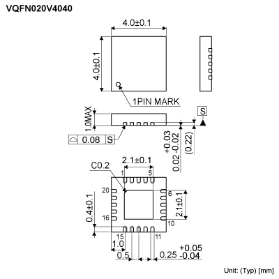
Product dimension image
Integrated Circuits (ICs)

BD9611MUV-E2

Active
Rohm Semiconductor

60V SYNCHRONOUS STEP-DOWN SWITCHING REGULATOR (CONTROLLER TYPE)

Deep-Dive with AI

Search across all available documentation for this part.

Product dimension image
Integrated Circuits (ICs)

BD9611MUV-E2

Active
Rohm Semiconductor

60V SYNCHRONOUS STEP-DOWN SWITCHING REGULATOR (CONTROLLER TYPE)

Technical Specifications

Parameters and characteristics for this part

SpecificationBD9611MUV-E2
Clock SyncTrue
Control FeaturesSoft Start, Frequency Control, Current Limit, Enable
Frequency - Switching [Max]500 kHz
Frequency - Switching [Min]50 kHz
FunctionStep-Down
Mounting TypeSurface Mount
Number of Outputs1
Operating Temperature [Max]105 °C
Operating Temperature [Min]-40 °C
Output ConfigurationPositive
Output Phases1
Output TypeTransistor Driver
Package / Case20-VFQFN Exposed Pad
Supplier Device PackageVQFN020V4040
Synchronous RectifierTrue
TopologyBuck
Voltage - Supply (Vcc/Vdd) [Max]56 V
Voltage - Supply (Vcc/Vdd) [Min]10 V

Pricing

Prices provided here are for design reference only. For realtime values and availability, please visit the distributors directly

DistributorPackageQuantity$
DigikeyCut Tape (CT) 1$ 3.34
10$ 2.17
100$ 1.51
500$ 1.23
1000$ 1.14
Digi-Reel® 1$ 3.34
10$ 2.17
100$ 1.51
500$ 1.23
1000$ 1.14
N/A 1578$ 3.32
Tape & Reel (TR) 2500$ 1.05
NewarkEach (Supplied on Cut Tape) 1$ 2.69
10$ 2.51
25$ 2.36
50$ 2.22
100$ 2.07
250$ 1.91
500$ 1.85
1000$ 1.79

Description

General part information

BD9611 Series

The BD9611MUV is a high-resistance, wide voltage input (10V to 56V), synchronous step-down switching regulator. BD9611MUV offers design flexibility through user-programmable functions such as soft-start, operating frequency, high-side current limit, and loop compensation. BD9611MUV uses voltage pulse width modulation, and drives 2 external N-channel FETs. The Under-Voltage Locked Output (EXUVLO) protection connected to its CTL terminal has high accuracy reference voltage. Its threshold voltage can be adjusted by the resistance ratio between VCC and GND as seen by pin CTL. BD9611MUV is safe for pre-biased outputs. It does not turn on the synchronous rectifier until the internal high-side FET has already started switching.

Documents

Technical documentation and resources

PCB Layout Techniques of Buck Converter

Schematic Design & Verification

Considerations for Power Inductors Used for Buck Converters

Schematic Design & Verification

Considering Polarity of Power Inductor to Reduce Radiated Emission of DC-DC converter

Schematic Design & Verification

UL94 Flame Classifications of Mold Compound

Environmental Data

θ<sub>JC</sub> and Ψ<sub>JT</sub>

Thermal Design

Anti-Whisker formation

Package Information

BD9611MUV Reference Circuits and Bomlist

Reference Design

Types of Capacitors Used for Output Smoothing of Switching Regulators and their Precautions

Schematic Design & Verification

Judgment Criteria of Thermal Evaluation

Thermal Design

SPICE Modeling Report - BD9611MUV : 60V Synchronous Step-down Switching Regulator (Controller Type)

Models

Power Supply Sequence Circuit with General Purpose Power Supply IC

Schematic Design & Verification

Snubber Circuit for Buck Converter IC

Schematic Design & Verification

Step-down DC-DC converter PCB layout EMC Design guide

Schematic Design & Verification

Efficiency of Buck Converter

Schematic Design & Verification

Precautions When Measuring the Rear of the Package with a Thermocouple

Thermal Design

Phase Compensation Design for Current Mode Buck Converter

Schematic Design & Verification

Simulation Guide for BD9611MUV / Frequency Response (ROHM Solution Simulator)

Simulations

Solder Joint Rate and Thermal Resistance of Exposed Pad

Thermal Design

Evaluation Board User's Guide

User's Guide

VQFN020V4040 Package Information

Package Information

Design Guide and Example of Stencil for Exposed Pad

Thermal Design

Buck DCDC application circuit example using BD9611MUV

Schematic Design & Verification

Factory Information

Manufacturing Data

Heat Dissipation Effect of Thermal Via in Exposed Pad Type Package

Thermal Design

θ<sub>JA</sub> and Ψ<sub>JT</sub>

Thermal Design

Suppression Method of Switching Noise Using Linear Regulator and Low Pass Filter

Schematic Design & Verification

How to Use the Thermal Resistance and Thermal Characteristics Parameters

Thermal Design

Cutting-Edge Web Simulation Tool "ROHM Solution Simulator" Capable of Complete Circuit Verification of Power Devices and Driver ICs

White Paper

Precautions for PCB Layout Regarding Common Mode Filters

Technical Article

Two-Resistor Model for Thermal Simulation

Thermal Design

Compliance with the ELV directive

Environmental Data

Calculation of Power Dissipation in Switching Circuit

Schematic Design & Verification

Considering Input Filter to Reduce Conducted Emissions by DCDC Converter

Schematic Design & Verification

Five Steps for Successful Thermal Design of IC

White Paper

Diode Selection Method for Asynchronous Converter

Schematic Design & Verification

The Important Points of Multi-layer Ceramic Capacitor Used in Buck Converter circuit

Schematic Design & Verification

Thermal Resistance

Thermal Design

PCB Layout Thermal Design Guide

Thermal Design

Method for Determining Constants of Peripheral Parts of Buck DC/DC Converter

Schematic Design & Verification

BD9611MUV Data Sheet

Data Sheet

Basics of Thermal Resistance and Heat Dissipation

Thermal Design

Resistor Value Table to set Output Voltage of Buck Converter IC

Schematic Design & Verification

Capacitor Calculation for Buck converter IC

Schematic Design & Verification

Overview of ROHM's Simulation Models(for ICs and Discrete Semiconductors)

Technical Article

PCB Layout Essential Check sheet for Switching Regulator

Schematic Design & Verification

How to Use the Two-Resistor Model

Thermal Design

Calculation of Power Loss (Synchronous)

Schematic Design & Verification

1ch Buck Switching Regulator BD9611MUV Phase Compensation Setting

Schematic Design & Verification

What Is Thermal Design

Thermal Design

Measurement Method for Phase Margin with Frequency Response Analyzer (FRA)

Schematic Design & Verification

Inductor Calculation for Buck converter IC

Schematic Design & Verification

Method for Calculating Junction Temperature from Transient Thermal Resistance Data

Thermal Design

Impedance Characteristics of Bypass Capacitor

Schematic Design & Verification

Three Steps for Successful Design of DC-DC Converters

White Paper