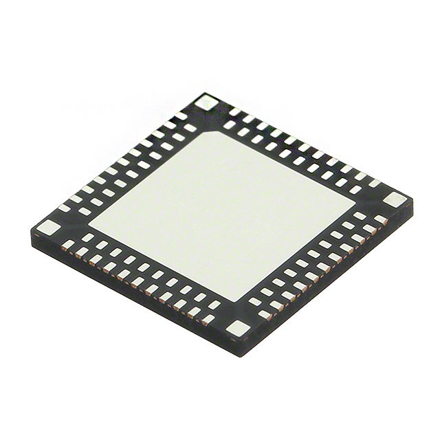
DAC3482IRKD25
ObsoleteDAC 2-CH SEGMENT 16-BIT 88-PIN WQFN EP T/R
Deep-Dive with AI
Search across all available documentation for this part.

DAC3482IRKD25
ObsoleteDAC 2-CH SEGMENT 16-BIT 88-PIN WQFN EP T/R
Deep-Dive with AI
Technical Specifications
Parameters and characteristics for this part
| Specification | DAC3482IRKD25 |
|---|---|
| Architecture | Current Source |
| Data Interface | LVDS - Parallel |
| Differential Output | True |
| INL/DNL (LSB) | 4 LSB, 2 LSB |
| Mounting Type | Surface Mount |
| Number of Bits | 16 |
| Operating Temperature [Max] | 85 °C |
| Operating Temperature [Min] | -40 °C |
| Output Type | Current - Unbuffered |
| Package / Case | 88-WQFN Exposed Pad |
| Reference Type | External, Internal |
| Settling Time | 10 ns |
| Supplier Device Package | 88-WQFN-MR (9x9) |
| Voltage - Supply, Analog [Max] | 3.46 V |
| Voltage - Supply, Analog [Min] | 3.14 V |
| Voltage - Supply, Digital [Max] | 1.32 V |
| Voltage - Supply, Digital [Min] | 1.14 V |
Pricing
Prices provided here are for design reference only. For realtime values and availability, please visit the distributors directly
| Distributor | Package | Quantity | $ | |
|---|---|---|---|---|
Description
General part information
DAC3482 Series
The DAC3482 is a very low power, high dynamic range, dual-channel, 16-bit digital-to-analog converter (DAC) with a sample rate as high as 1.25GSPS.
The device includes features that simplify the design of complex transmit architectures: 2x to 16x digital interpolation filters with over 90dB of stop-band attenuation simplify the data interface and reconstruction filters. A complex mixer allows flexible carrier placement. A high-performance low jitter clock multiplier simplifies clocking of the device without significant impact on the dynamic range. The digital Quadrature Modulator Correction (QMC) enables complete IQ compensation for gain, offset, phase, and group delay between channels in direct up-conversion applications.
Digital data is input to the device through a flexible LVDS data bus with on-chip termination. Data can be input either word-wide or byte-wide. The device includes a FIFO, data pattern checker and parity test to ease the input interface. The interface also allows full synchronization of multiple devices.
Documents
Technical documentation and resources


