Deep-Dive with AI
Search across all available documentation for this part.

Deep-Dive with AI
Technical Specifications
Parameters and characteristics for this part
| Specification | ADF4151BCPZ-RL7 |
|---|---|
| Differential - Input:Output | Yes/No |
| Frequency - Max [Max] | 3.5 GHz |
| Input | CMOS, TTL |
| Mounting Type | Surface Mount |
| Number of Circuits | 1 |
| Operating Temperature [Max] | 85 °C |
| Operating Temperature [Min] | -40 °C |
| Output | Clock |
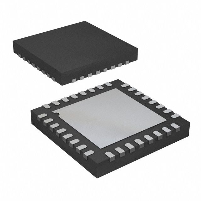
| Package / Case | 32-WFQFN Exposed Pad, CSP |
| PLL | True |
| Ratio - Input:Output | 2:1 |
| Supplier Device Package | 32-LFCSP-WQ (5x5) |
| Voltage - Supply [Max] | 3.6 V |
| Voltage - Supply [Min] | 3 V |
Pricing
Prices provided here are for design reference only. For realtime values and availability, please visit the distributors directly
| Distributor | Package | Quantity | $ | |
|---|---|---|---|---|
| Digikey | Tape & Reel (TR) | 1500 | $ 4.42 | |
Description
General part information
ADF4151 Series
The ADF4151 allows implementation of fractional-N or integer-N phase-locked loop (PLL) frequency synthesizers if used with an external voltage controlled oscillator (VCO), loop filter, and external reference frequency.The ADF4151 is used with external VCO parts and is footprint and software compatible with theADF4350. The part consists of a low noise digital phase frequency detector (PFD), a precision charge pump, and a programmable reference divider. There is a Σ-Δ based fractional interpolator to allow programmable fractional-N division. The INT, FRAC, and MOD registers define an overall N divider [N = (INT + (FRAC/MOD))]. The RF output phase is programmable for applications that require a particular phase relationship between the output and the reference. The ADF4151 also features cycle slip reduction circuitry, leading to faster lock times without the need for modifications to the loop filter.Control of all the on-chip registers is through a simple 3-wire interface. The device operates with a power supply ranging from 3.0 V to 3.6 V that can be powered down when not in use.The ADF4151 is available in a 5 mm × 5 mm package.ApplicationsWireless infrastructure (W-CDMA, TD-SCDMA, WiMax,GSM, PCS, DCS, DECT)Test equipmentWireless LANs, CATV equipmentClock generation


