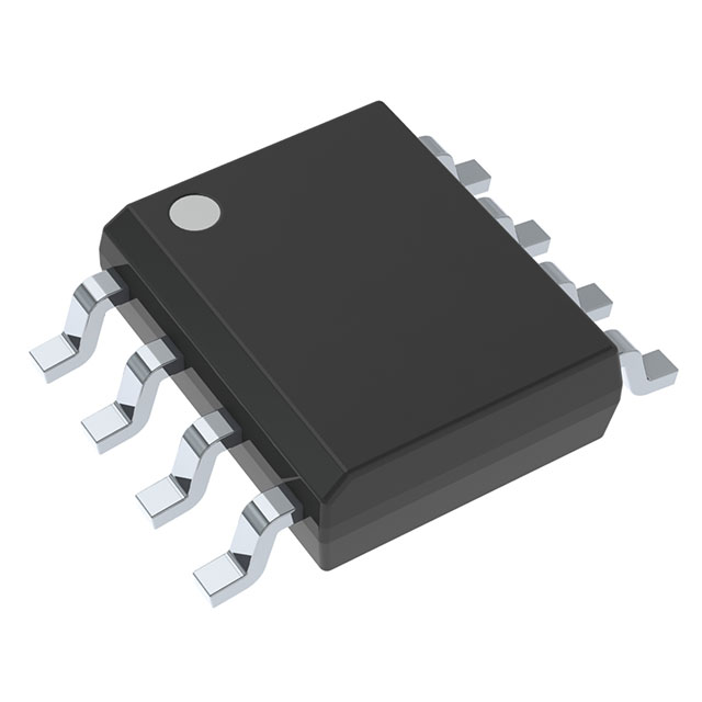
LM9061M/NOPB
Active7-V TO 26-V HIGH SIDE PROTECTION CONTROLLER
Deep-Dive with AI
Search across all available documentation for this part.

LM9061M/NOPB
Active7-V TO 26-V HIGH SIDE PROTECTION CONTROLLER
Technical Specifications
Parameters and characteristics for this part
| Specification | LM9061M/NOPB |
|---|---|
| Channel Type | Single |
| Driven Configuration | High-Side |
| Gate Type | N-Channel MOSFET |
| Input Type | Non-Inverting |
| Logic Voltage - VIL, VIH [custom] | 3.5 V |
| Logic Voltage - VIL, VIH [custom] | 1.5 V |
| Mounting Type | Surface Mount |
| Number of Drivers | 1 |
| Operating Temperature [Max] | 150 °C |
| Operating Temperature [Min] | -40 °C |
| Package / Case | 8-SOIC |
| Package / Case [x] | 0.154 in |
| Package / Case [y] | 3.9 mm |
| Supplier Device Package | 8-SOIC |
| Voltage - Supply [Max] | 26 V |
| Voltage - Supply [Min] | 7 V |
Pricing
Prices provided here are for design reference only. For realtime values and availability, please visit the distributors directly
| Distributor | Package | Quantity | $ | |
|---|---|---|---|---|
| Digikey | Tube | 1 | $ 4.19 | |
| 10 | $ 3.76 | |||
| 95 | $ 3.08 | |||
| 285 | $ 2.93 | |||
| 570 | $ 2.63 | |||
| 1045 | $ 2.21 | |||
| 2565 | $ 2.10 | |||
| Texas Instruments | TUBE | 1 | $ 2.70 | |
| 100 | $ 2.37 | |||
| 250 | $ 1.66 | |||
| 1000 | $ 1.34 | |||
Description
General part information
LM9061-Q1 Series
The LM9061 family consists of charge-pump devices which provides the gate drive to an external power MOSFET of any size configured as a high-side driver or switch. This includes multiple parallel connected MOSFETs for very high current applications. A CMOS logic-compatible ON and OFF input controls the output gate drive voltage. In the ON state, the charge pump voltage, which is well above the available VCCsupply, is directly applied to the gate of the MOSFET. A built-in 15-V Zener clamps the maximum gate to source voltage of the MOSFET. When commanded OFF a 110-µA current sink discharges the gate capacitances of the MOSFET for a gradual turnoff characteristic to minimize the duration of inductive load transient voltages and further protect the power MOSFET.
Lossless protection of the power MOSFET is a key feature of the LM9061. The voltage drop (VDS) across the power device is continually monitored and compared against an externally programmable threshold voltage. A small current-sensing resistor in series with the load, which causes a loss of available energy, is not required for the protection circuitry. If the VDSvoltage, due to excessive load current, exceeds the threshold voltage, the output is latched OFF in a more gradual fashion (through a 10-µA output current sink) after a programmable delay time interval.
The LM9061 family consists of charge-pump devices which provides the gate drive to an external power MOSFET of any size configured as a high-side driver or switch. This includes multiple parallel connected MOSFETs for very high current applications. A CMOS logic-compatible ON and OFF input controls the output gate drive voltage. In the ON state, the charge pump voltage, which is well above the available VCCsupply, is directly applied to the gate of the MOSFET. A built-in 15-V Zener clamps the maximum gate to source voltage of the MOSFET. When commanded OFF a 110-µA current sink discharges the gate capacitances of the MOSFET for a gradual turnoff characteristic to minimize the duration of inductive load transient voltages and further protect the power MOSFET.
Documents
Technical documentation and resources


