Deep-Dive with AI
Search across all available documentation for this part.

Technical Specifications
Parameters and characteristics for this part
| Specification | ADN2805ACPZ-RL7 |
|---|---|
| Differential - Input:Output [custom] | True |
| Differential - Input:Output [custom] | True |
| Frequency - Max [Max] | 1.25 GHz |
| Input | CML |
| Main Purpose | SONET/SDH |
| Mounting Type | Surface Mount |
| Number of Circuits | 1 |
| Operating Temperature [Max] | 85 °C |
| Operating Temperature [Min] | -40 °C |
| Output | LVDS |
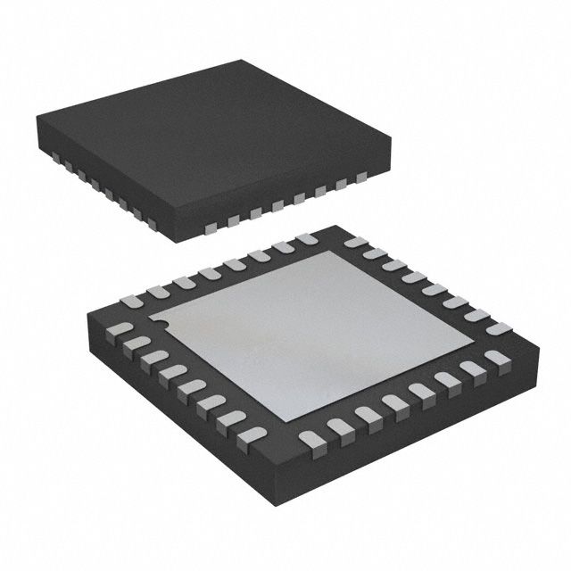
| Package / Case | 32-WFQFN Exposed Pad, CSP |
| PLL | True |
| Ratio - Input:Output [custom] | 1:2 |
| Supplier Device Package | 32-LFCSP-WQ (5x5) |
| Voltage - Supply [Max] | 3.6 V |
| Voltage - Supply [Min] | 3 V |
Pricing
Prices provided here are for design reference only. For realtime values and availability, please visit the distributors directly
| Distributor | Package | Quantity | $ | |
|---|---|---|---|---|
Description
General part information
ADN2805 Series
The ADN2805 provides the receiver functions of quantization and clock and data recovery for 1.25 Gbps. The ADN2805 automatically locks to all data rates without the need for an external reference clock or programming. All SONET jitter requirements are met, including jitter transfer, jitter generation, and jitter tolerance.All specifications are specified for −40°C to +85°C ambient temperature, unless otherwise noted. The ADN2805 is available in a compact 5 mm × 5 mm 32-lead LFCSP.ApplicationsGbE line card


