Deep-Dive with AI
Search across all available documentation for this part.

Deep-Dive with AI
Technical Specifications
Parameters and characteristics for this part
| Specification | SY100EL90VZC |
|---|---|
| Channel Type | Unidirectional |
| Channels per Circuit | 3 |
| Input Signal | ECL, LVECL |
| Mounting Type | Surface Mount |
| Number of Circuits | 1 |
| Operating Temperature [Max] | 85 C |
| Operating Temperature [Min] | 0 °C |
| Output Signal | LVPECL, PECL |
| Output Type | Differential |
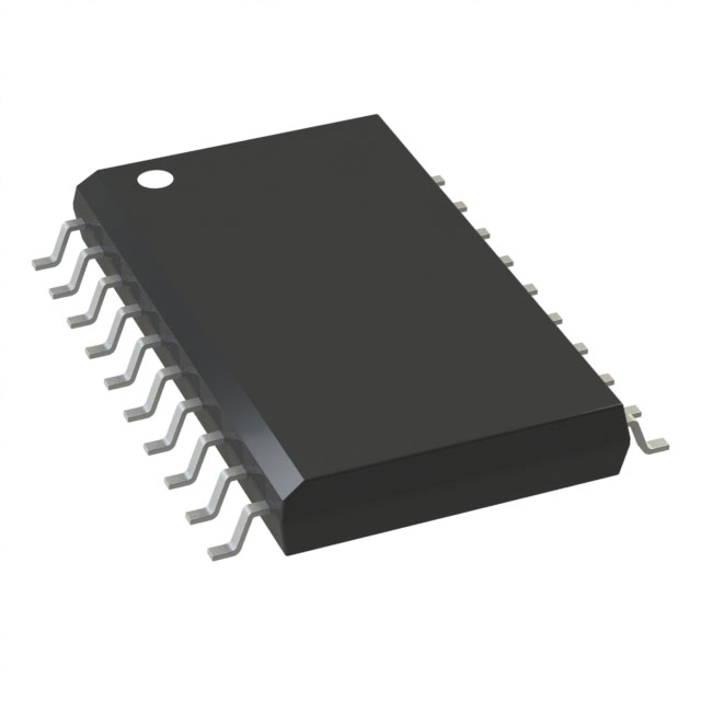
| Package / Case | 20-SOIC |
| Package / Case [y] | 0.295 in |
| Package / Case [y] | 7.5 mm |
| Supplier Device Package | 20-SOIC |
| Translator Type | Mixed Signal |
Pricing
Prices provided here are for design reference only. For realtime values and availability, please visit the distributors directly
| Distributor | Package | Quantity | $ | |
|---|---|---|---|---|
| Digikey | Tube | 228 | $ 4.69 | |
Description
General part information
SY100EL90 Series
The SY100EL90V is a triple ECL/LVECL-to-PECL/LVPECL translator. The device can translate over all combinations of supply voltages: -5V ECL to 5V PECL, -5V ECL to 3.3V LVPECL, -3.3V LVECL to 5V PECL or -3.3V LVECL to 3.3V LVPECL.A VBB output is provided for interfacing with single ended ECL signals at the input. If a single ended input is to be used, the VBB output should be connected to the D input. The active signal would then drive the D input. When used, the VBBoutput should be bypassed to via a 0.01µF capacitor. The VBB output is designed to act as the switching reference for the EL90V under single ended input switching conditions. As a result this pin can only source/sink up to 0.5mA of current.
To accomplish the level translation the EL90V requires three power rails. The VCC supply should be connected to the positive supply, and the VEE pin should be connected to the negative power supply. The GND pins as expected are connected to the system ground plane. Both VEE and VCC should be bypassed to ground via 0.01µF capacitors.Under open input conditions, the D input will be biased at VCC/2 and the D input will be pulled to VEE. This condition will force the Q output to a LOW, ensuring stability.
Documents
Technical documentation and resources


