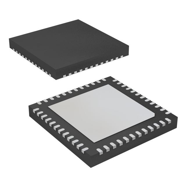
ADS41B25IRGZR
Active12-BIT, 125-MSPS ANALOG-TO-DIGITAL CONVERTER (ADC)
Deep-Dive with AI
Search across all available documentation for this part.

ADS41B25IRGZR
Active12-BIT, 125-MSPS ANALOG-TO-DIGITAL CONVERTER (ADC)
Technical Specifications
Parameters and characteristics for this part
| Specification | ADS41B25IRGZR |
|---|---|
| Architecture | Pipelined |
| Configuration | S/H-ADC |
| Data Interface | LVDS - Parallel, Parallel |
| Input Type | Differential |
| Mounting Type | Surface Mount |
| Number of A/D Converters | 1 |
| Number of Bits | 12 bits |
| Number of Inputs | 1 |
| Operating Temperature [Max] | 85 °C |
| Operating Temperature [Min] | -40 °C |
| Package / Case | 48-VFQFN Exposed Pad |
| Ratio - S/H:ADC | 1:1 |
| Reference Type | Internal |
| Sampling Rate (Per Second) | 125 M |
| Supplier Device Package | 48-VQFN (7x7) |
| Voltage - Supply, Analog [Max] | 1.9 V |
| Voltage - Supply, Analog [Min] | 1.7 V |
| Voltage - Supply, Digital [Max] | 1.9 V |
| Voltage - Supply, Digital [Min] | 1.7 V |
Pricing
Prices provided here are for design reference only. For realtime values and availability, please visit the distributors directly
| Distributor | Package | Quantity | $ | |
|---|---|---|---|---|
| Digikey | Tape & Reel (TR) | 2500 | $ 33.70 | |
| Texas Instruments | LARGE T&R | 1 | $ 41.17 | |
| 100 | $ 36.60 | |||
| 250 | $ 30.09 | |||
| 1000 | $ 26.91 | |||
Description
General part information
ADS41B25 Series
The ADS41B25 is a member of the ultralow-power ADS4xxx analog-to-digital converter (ADC) family, featuring integrated analog input buffers. This device uses innovative design techniques to achieve high dynamic performance, while consuming extremely low power. The analog input pins have buffers, with the benefits of constant performance and input impedance across a wide frequency range. The device is well-suited for multi-carrier, wide bandwidth communications applications such as PA linearization.
The ADS41B25 has features such as digital gain and offset correction. The gain option can be used to improve SFDR performance at lower full-scale input ranges, especially at high input frequencies. The integrated dc offset correction loop can be used to estimate and cancel the ADC offset. At lower sampling rates, the ADC automatically operates at scaled-down power with no loss in performance.
The device supports both double data rate (DDR) low-voltage differential signaling (LVDS) and parallel CMOS digital output interfaces. The low data rate of the DDR LVDS interface (maximum 500MBPS) makes it possible to use low-cost field-programmable gate array (FPGA)-based receivers. The device has a low-swing LVDS mode that can be used to further reduce the power consumption. The strength of the LVDS output buffers can also be increased to support 50Ω differential termination.
Documents
Technical documentation and resources


