Catalog
12-Bit, 125-MSPS Analog-to-Digital Converter (ADC)
Key Features
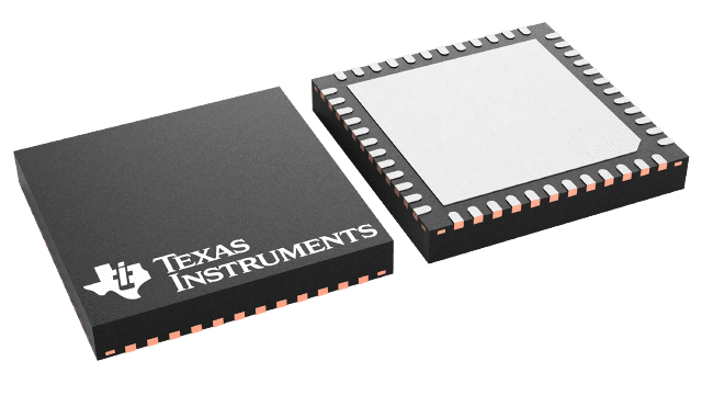
• Resolution: 12-Bit, 125MSPSIntegrated High-ImpedanceAnalog Input Buffer:Input Capacitance at dc: 3.5pFInput Resistance at dc: 10kΩMaximum Sample Rate: 125MSPSUltralow Power:1.8V Analog Power: 114mW3.3V Buffer Power: 96mWI/O Power: 100mW (DDR LVDS)High Dynamic Performance:SNR: 68.3dBFS at 170MHzSFDR: 87dBc at 170MHzOutput Interface:Double Data Rate (DDR) LVDS with Programmable Swing and Strength:Standard Swing: 350mVLow Swing: 200mVDefault Strength: 100Ω Termination2x Strength: 50Ω Termination1.8V Parallel CMOS Interface Also SupportedProgrammable Gain for SNR/SFDR Trade-OffDC Offset CorrectionSupports Low Input Clock AmplitudePackage: QFN-48 (7mm × 7mm)PowerPAD is a trademark of Texas Instruments, Incorporated.All other trademarks are the property of their respective owners.Resolution: 12-Bit, 125MSPSIntegrated High-ImpedanceAnalog Input Buffer:Input Capacitance at dc: 3.5pFInput Resistance at dc: 10kΩMaximum Sample Rate: 125MSPSUltralow Power:1.8V Analog Power: 114mW3.3V Buffer Power: 96mWI/O Power: 100mW (DDR LVDS)High Dynamic Performance:SNR: 68.3dBFS at 170MHzSFDR: 87dBc at 170MHzOutput Interface:Double Data Rate (DDR) LVDS with Programmable Swing and Strength:Standard Swing: 350mVLow Swing: 200mVDefault Strength: 100Ω Termination2x Strength: 50Ω Termination1.8V Parallel CMOS Interface Also SupportedProgrammable Gain for SNR/SFDR Trade-OffDC Offset CorrectionSupports Low Input Clock AmplitudePackage: QFN-48 (7mm × 7mm)PowerPAD is a trademark of Texas Instruments, Incorporated.All other trademarks are the property of their respective owners.
Description
AI
The ADS41B25 is a member of the ultralow-power ADS4xxx analog-to-digital converter (ADC) family, featuring integrated analog input buffers. This device uses innovative design techniques to achieve high dynamic performance, while consuming extremely low power. The analog input pins have buffers, with the benefits of constant performance and input impedance across a wide frequency range. The device is well-suited for multi-carrier, wide bandwidth communications applications such as PA linearization.
The ADS41B25 has features such as digital gain and offset correction. The gain option can be used to improve SFDR performance at lower full-scale input ranges, especially at high input frequencies. The integrated dc offset correction loop can be used to estimate and cancel the ADC offset. At lower sampling rates, the ADC automatically operates at scaled-down power with no loss in performance.
The device supports both double data rate (DDR) low-voltage differential signaling (LVDS) and parallel CMOS digital output interfaces. The low data rate of the DDR LVDS interface (maximum 500MBPS) makes it possible to use low-cost field-programmable gate array (FPGA)-based receivers. The device has a low-swing LVDS mode that can be used to further reduce the power consumption. The strength of the LVDS output buffers can also be increased to support 50Ω differential termination.
The device is available in a compact QFN-48 package and is specified over the industrial temperature range (–40°C to +85°C).


