Deep-Dive with AI
Search across all available documentation for this part.

Deep-Dive with AI
Technical Specifications
Parameters and characteristics for this part
| Specification | 5962-8853901EA |
|---|---|
| -3db Bandwidth | 1 MHz |
| Amplifier Type | Instrumentation |
| Current - Input Bias | 1 µA |
| Current - Supply | 5 mA |
| Gain Bandwidth Product | 1 MHz |
| Mounting Type | Through Hole |
| Number of Circuits | 1 |
| Operating Temperature [Max] | 125 °C |
| Operating Temperature [Min] | -55 °C |
| Package / Case | 7.62 mm, 0.3 in |
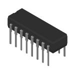
| Package / Case | 16-CDIP |
| Slew Rate | 5 V/çs |
| Supplier Device Package | 16-CDIP |
| Voltage - Input Offset | 1 mV |
| Voltage - Supply Span (Max) [Max] | 36 V |
| Voltage - Supply Span (Min) [Min] | 12 V |
Pricing
Prices provided here are for design reference only. For realtime values and availability, please visit the distributors directly
| Distributor | Package | Quantity | $ | |
|---|---|---|---|---|
Description
General part information
5962-8853901 Series
The AD524 is a precision monolithic instrumentation amplifier designed for data acquisition applications requiring high accuracy under worst-case operating conditions. An outstanding combination of high linearity, high common-mode rejection, low offset voltage drift, and low noise makes the AD524 suitable for use in many data acquisition systems. The AD524 has an output offset voltage drift of less than 25 μV/°C, input offset voltage drift of less than 0.5 μV/°C, CMR above 90 dB at unity gain (120 dB at G = 1000), and maximum nonlinearity of 0.003% at G = 1. The gain bandwidth product of the AD524 is 25 kHz (G = 1000). The output slew rate of 5 V/μs and settling time of 15 μs to 0.01% for gains of 1 to 100, makes it suitable for high speed data acquisition systems.As a complete amplifier, the AD524 does not require any external components for fixed gains of 1, 10, 100, and 1000. For other gain settings between 1 and 1000, only a single resistor is required. The AD524 input is fully protected for both power-on and power-off fault conditions. The AD524 is available in four versions of accuracy and operating temperature range. The economical A grade, the low drift B grade, and lower drift, higher linearity C grade are specified from −25°C to +85°C. The S grade guarantees performance to specification over the extended temperature range −55°C to +125°C. The AD524 is available in a 16-lead ceramic DIP, 16-lead SBDIP, 16‑lead SOIC wide packages, and 20-terminal leadless chip carrier.PRODUCT HIGHLIGHTSGuaranteed low offset voltage, low offset voltage drift, and low noise for precision high gain applications.Functionally complete with pin programmable gains of 1, 10, 100, and 1000, and single resistor-programmable for any gain.Input and output offset nulling terminals are provided for high precision applications and to minimize offset voltage changes in gain ranging applications.Input protected for both power-on and power-off fault conditions.Superior dynamic performance with a gain bandwidth product of 25 MHz, full power response of 75 kHz and a settling time of 15 μs to 0.01% of a 20 V step (G = 100).
Documents
Technical documentation and resources


