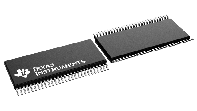
SN74GTL16612DGGR
Active18-BIT LVTTL-TO-GTL/GTL+ UNIVERSAL BUS TRANSCEIVERS
Deep-Dive with AI
Search across all available documentation for this part.

SN74GTL16612DGGR
Active18-BIT LVTTL-TO-GTL/GTL+ UNIVERSAL BUS TRANSCEIVERS
Technical Specifications
Parameters and characteristics for this part
| Specification | SN74GTL16612DGGR |
|---|---|
| Current - Output High, Low [custom] | 64 mA |
| Current - Output High, Low [custom] | 32 mA |
| Mounting Type | Surface Mount |
| Number of Circuits | 18 Bit |
| Operating Temperature [Max] | 85 °C |
| Operating Temperature [Min] | -40 °C |
| Package / Case | 6.1 mm |
| Package / Case | 0.24 in |
| Package / Case | 56-TFSOP |
| Supplier Device Package | 56-TSSOP |
| Voltage - Supply [Max] | 3.45 V |
| Voltage - Supply [Min] | 3.15 V |
Pricing
Prices provided here are for design reference only. For realtime values and availability, please visit the distributors directly
| Distributor | Package | Quantity | $ | |
|---|---|---|---|---|
| Digikey | Cut Tape (CT) | 1 | $ 9.87 | |
| Digi-Reel® | 1 | $ 9.87 | ||
| Tape & Reel (TR) | 2000 | $ 5.84 | ||
| Texas Instruments | LARGE T&R | 1 | $ 8.00 | |
| 100 | $ 6.52 | |||
| 250 | $ 5.13 | |||
| 1000 | $ 4.35 | |||
Description
General part information
SN74GTL16612 Series
The 'GTL16612 devices are 18-bit UBT™ transceivers that provide LVTTL-to-GTL/GTL+ and GTL/GTL+-to-LVTTL signal-level translation. They combine D-type flip-flops and D-type latches to allow for transparent, latched, clocked, and clock-enabled modes of data transfer identical to the '16601 function. The devices provide an interface between cards operating at LVTTL logic levels and a backplane operating at GTL/GTL+ signal levels. Higher-speed operation is a direct result of the reduced output swing (<1 V), reduced input threshold levels, and OEC™ circuitry.
The user has the flexibility of using these devices at either GTL (VTT= 1.2 V and VREF= 0.8 V) or the preferred higher noise margin GTL+ (VTT= 1.5 V and VREF= 1 V) signal levels. GTL+ is the Texas Instruments derivative of the Gunning Transceiver Logic (GTL) JEDEC standard JESD 8-3. The B port normally operates at GTL or GTL+ signal levels, while the A-port and control inputs are compatible with LVTTL logic levels and are 5-V tolerant. VREFis the reference input voltage for the B port.
VCC(5 V) supplies the internal and GTL circuitry while VCC(3.3 V) supplies the LVTTL output buffers.
Documents
Technical documentation and resources


