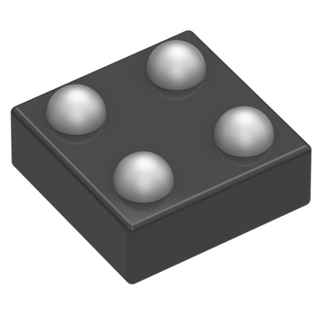
ADP191ACBZ-R7
ActiveLOGIC CONTROLLED, HIGH-SIDE POWER SWITCHES
Deep-Dive with AI
Search across all available documentation for this part.

ADP191ACBZ-R7
ActiveLOGIC CONTROLLED, HIGH-SIDE POWER SWITCHES
Technical Specifications
Parameters and characteristics for this part
| Specification | ADP191ACBZ-R7 |
|---|---|
| Current - Output (Max) [Max] | 500 mA |
| Features | Slew Rate Controlled, Load Discharge |
| Input Type | Non-Inverting |
| Interface | On/Off |
| Mounting Type | Surface Mount |
| Number of Outputs | 1 |
| Operating Temperature [Max] | 125 ¯C |
| Operating Temperature [Min] | -40 °C |
| Output Configuration | High Side |
| Output Type | P-Channel |
| Package / Case | WLCSP, 4-WFBGA |
| Ratio - Input:Output [custom] | 1:1 |
| Rds On (Typ) | 80 mOhm |
| Supplier Device Package | 4-WLCSP (0.76x0.76) |
| Switch Type | General Purpose |
| Voltage - Load [Max] | 3.6 V |
| Voltage - Load [Min] | 1.1 V |
| Voltage - Supply (Vcc/Vdd) | False |
Pricing
Prices provided here are for design reference only. For realtime values and availability, please visit the distributors directly
| Distributor | Package | Quantity | $ | |
|---|---|---|---|---|
| Digikey | Cut Tape (CT) | 1 | $ 2.01 | |
| 10 | $ 1.28 | |||
| 25 | $ 1.09 | |||
| 100 | $ 0.87 | |||
| 250 | $ 0.77 | |||
| 500 | $ 0.70 | |||
| 1000 | $ 0.65 | |||
| Digi-Reel® | 1 | $ 2.01 | ||
| 10 | $ 1.28 | |||
| 25 | $ 1.09 | |||
| 100 | $ 0.87 | |||
| 250 | $ 0.77 | |||
| 500 | $ 0.70 | |||
| 1000 | $ 0.65 | |||
| Tape & Reel (TR) | 3000 | $ 0.58 | ||
| 6000 | $ 0.55 | |||
| 9000 | $ 0.53 | |||
| 15000 | $ 0.51 | |||
Description
General part information
ADP191 Series
TheADP190/ ADP191 are high-side load switches designed for operation from 1.2 V to 3.6 V. These load switches provide power domain isolation for extended power battery life. The devices contain a low on-resistance P-channel MOSFET that supports more than 500 mA of continuous current and minimizes power loss. The low 2 μA (maximum) of ground current and ultralow shutdown current make the ADP190 / ADP191 ideal for battery-operated portable equipment. The built-in level shifter for enable logic makes the ADP190 / ADP191 compatible with modern processors and GPIO controllers.The ADP191 controls the turn-on slew rate of the switch to reduce the input inrush current. The ADP191 also incorporates an internal output discharge resistor to discharge the output capacitance when the ADP191 output is disabled.Beyond operating performance, the ADP190 / ADP191 occupy minimal printed circuit board (PCB) space with an area less than 0.64 mm2and a height of 0.60 mm. It is available in an ultrasmall 0.8 mm × 0.8 mm, 4-ball, 0.4 mm pitch WLCSP.APPLICATIONSMobile phonesDigital cameras and audio devicesPortable and battery-powered equipment


