Deep-Dive with AI
Search across all available documentation for this part.

Deep-Dive with AI
Technical Specifications
Parameters and characteristics for this part
| Specification | AD5336BRUZ-REEL |
|---|---|
| Architecture | String DAC |
| Data Interface | Parallel |
| Differential Output | False |
| INL/DNL (LSB) | 0.5 LSB, 0.05 LSB |
| Mounting Type | Surface Mount |
| Number of Bits [custom] | 10 |
| Number of D/A Converters | 4 |
| Operating Temperature [Max] | 105 ░C |
| Operating Temperature [Min] | -40 °C |
| Output Type | Voltage - Buffered |
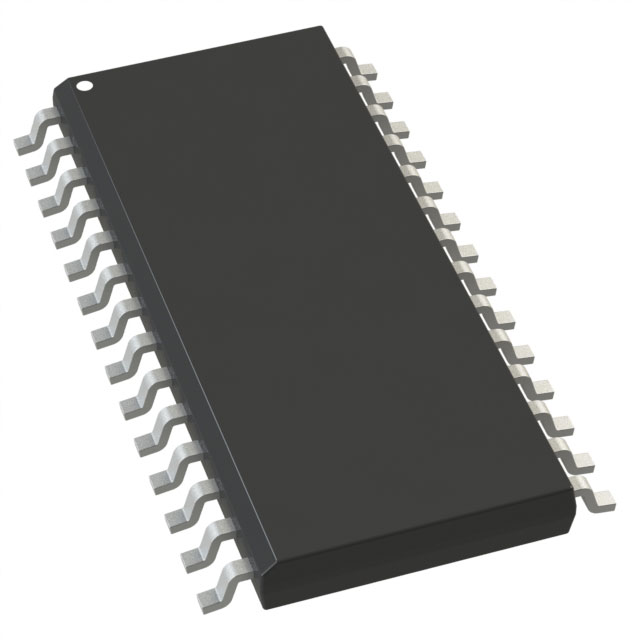
| Package / Case | 28-TSSOP |
| Package / Case | 0.173 in |
| Package / Case [y] | 4.4 mm |
| Reference Type | External |
| Settling Time | 9 µs |
| Supplier Device Package | 28-TSSOP |
| Voltage - Supply, Analog [Max] | 5.5 V |
| Voltage - Supply, Analog [Min] | 2.5 V |
| Voltage - Supply, Digital [Max] | 5.5 V |
| Voltage - Supply, Digital [Min] | 2.5 V |
Pricing
Prices provided here are for design reference only. For realtime values and availability, please visit the distributors directly
| Distributor | Package | Quantity | $ | |
|---|---|---|---|---|
Description
General part information
AD5336 Series
The AD5334 / AD5335 / AD5336 / AD5344 are quad 8-,10-,and 12-bit DACs. They operate from a 2.5 V to 5.5 V supply consuming just 500 µA at 3 V, and feature a power-down mode that further reduces the current to 80 nA. These devices incorporate an on-chip output buffer that can drive the output to both supply rails.The AD5334 / AD5335 / AD5336 / AD5344 have a parallel interface. CS selects the device and data is loaded into the input registers on the rising edge ofWR.The GAIN pin on the AD5334 and AD5336 allows the output range to be set at 0 V to VREFor 0 V to 2 × VREF.Input data to the DACs is double-buffered, allowing simultaneous update of multiple DACs in a system using theLDACpin.On the AD5334, AD5335 and AD5336 an asynchronousCLRinput is also provided. This resets the contents of the Input Register and the DAC Register to all zeros. These devices also incorporate a power-on-reset circuit that ensures that the DAC output powers on to 0 V and remains there until valid data is written to the device.The AD5334 / AD5335 / AD5336 / AD5344 are available in Thin Shrink Small Outline Packages (TSSOP).PRODUCT HIGHLIGHTSAvailable in a 28-lead TSSOP packageLow power, single supply operation from 2.5 V to 5.5 V supplyConsumes 1.5 mW at 3 V and 3 mW at 5 VOn-chip ouput buffer can drive output to both supply railsProgrammable output range 0-VREFor 0-2VREF(via GAIN pin)APPLICATIONSPortable Battery-Powered InstrumentsDigital Gain and Offset AdjustmentProgrammable Voltage and Current SourcesProgrammable AttenuatorsIndustrial Process Control
Documents
Technical documentation and resources


