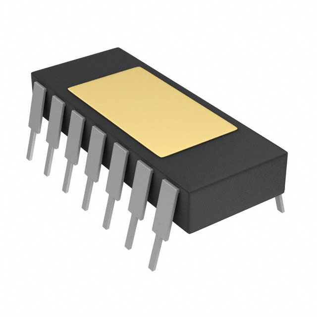
DAC811BH
LTB12-BIT DIGITAL-TO-ANALOG CONVERTER W/PARALLEL INTERFACE
Deep-Dive with AI
Search across all available documentation for this part.

DAC811BH
LTB12-BIT DIGITAL-TO-ANALOG CONVERTER W/PARALLEL INTERFACE
Deep-Dive with AI
Technical Specifications
Parameters and characteristics for this part
| Specification | DAC811BH |
|---|---|
| Architecture | R-2R |
| Data Interface | Parallel |
| Differential Output | False |
| INL/DNL (LSB) | 0.25 LSB, 0.125 LSB |
| Mounting Type | Through Hole |
| Number of Bits | 12 bits |
| Operating Temperature [Max] | 85 °C |
| Operating Temperature [Min] | -25 °C |
| Output Type | Voltage - Buffered |
| Package / Case | 28-CDIP Window |
| Package / Case | 0.6 in |
| Package / Case | 15.24 mm |
| Reference Type | Internal |
| Settling Time | 4 µs |
| Supplier Device Package | 28-CDIP |
| Voltage - Supply, Analog [Max] | 16.5 V |
| Voltage - Supply, Analog [Min] | -11.4 V |
| Voltage - Supply, Digital | 5 V |
DAC811 Series
12-bit Digital-to-Analog Converter w/Parallel Interface
| Part | Operating Temperature [Max] | Operating Temperature [Min] | Supplier Device Package | Reference Type | INL/DNL (LSB) | Voltage - Supply, Digital | Number of Bits | Differential Output | Settling Time | Mounting Type | Voltage - Supply, Analog [Min] | Voltage - Supply, Analog [Max] | Architecture | Output Type | Data Interface | Package / Case | Package / Case | Package / Case | Package / Case [x] | Package / Case [y] |
|---|---|---|---|---|---|---|---|---|---|---|---|---|---|---|---|---|---|---|---|---|
Texas Instruments | 70 °C | 0 °C | 28-PDIP | Internal | 0.25 LSB 0.5 LSB | 5 V | 12 bits | 4 µs | Through Hole | -11.4 V | 16.5 V | R-2R | Voltage - Buffered | Parallel | 28-DIP | 0.6 in | 15.24 mm | |||
Texas Instruments | 70 °C | 0 °C | 28-SOIC | Internal | 0.25 LSB 0.5 LSB | 5 V | 12 bits | 4 µs | Surface Mount | -11.4 V | 16.5 V | R-2R | Voltage - Buffered | Parallel | 28-SOIC | 0.295 in | 7.5 mm | |||
Texas Instruments | 70 °C | 0 °C | 28-PDIP | Internal | 0.25 LSB 0.5 LSB | 5 V | 12 bits | 4 µs | Through Hole | -11.4 V | 16.5 V | R-2R | Voltage - Buffered | Parallel | 28-DIP | 0.6 in | 15.24 mm | |||
Texas Instruments | 70 °C | 0 °C | 28-PDIP | Internal | 0.125 LSB 0.25 LSB | 5 V | 12 bits | 4 µs | Through Hole | -11.4 V | 16.5 V | R-2R | Voltage - Buffered | Parallel | 28-DIP | 0.6 in | 15.24 mm | |||
Texas Instruments | 70 °C | 0 °C | 28-SOIC | Internal | 0.125 LSB 0.25 LSB | 5 V | 12 bits | 4 µs | Surface Mount | -11.4 V | 16.5 V | R-2R | Voltage - Buffered | Parallel | 28-SOIC | 0.295 in | 7.5 mm | |||
Texas Instruments | 85 °C | -25 °C | 28-CDIP | Internal | 0.125 LSB 0.25 LSB | 5 V | 12 bits | 4 µs | Through Hole | -11.4 V | 16.5 V | R-2R | Voltage - Buffered | Parallel | 28-CDIP Window | 0.6 in | 15.24 mm | |||
Texas Instruments | 70 °C | 0 °C | 28-SOIC | Internal | 0.25 LSB 0.5 LSB | 5 V | 12 bits | 4 µs | Surface Mount | -11.4 V | 16.5 V | R-2R | Voltage - Buffered | Parallel | 28-SOIC | 0.295 in | 7.5 mm |
Pricing
Prices provided here are for design reference only. For realtime values and availability, please visit the distributors directly
| Distributor | Package | Quantity | $ | |
|---|---|---|---|---|
| Digikey | Tube | 12 | $ 82.61 | |
| Texas Instruments | TUBE | 1 | $ 99.99 | |
| 100 | $ 88.88 | |||
| 250 | $ 73.06 | |||
| 1000 | $ 65.35 | |||
Description
General part information
DAC811 Series
The DAC811 is a complete, single-chip integrated-circuit, microprocessor-compatible, 12-bit digital-to-analog converter. The chip combines a precision voltage reference, microcomputer interface logic, and double-buffered latch, in a 12-bit D/A converter with a voltage output amplifier. Fast current switches and a laser-trimmed thin-film resistor network provide a highly accurate and fast D/A converter.
Microcomputer interfacing is facilitated by a double-buffered latch. The input latch is divided into three 4-bit nibbles to permit interfacing to 4-, 8-, 12-, or 16-bit buses and to handle right-or left-justified data. The 12-bit data in the input latches is transferred to the D/A latch to hold the output value.
Input gating logic is designed so that loading the last nibble or byte of data can be accomplished simultaneously with the transfer of data (previously stored in adjacent latches) from adjacent input latches to the D/A latch. This feature avoids spurious analog output values while using an interface technique that saves computer instructions.
Documents
Technical documentation and resources


