Deep-Dive with AI
Search across all available documentation for this part.

Deep-Dive with AI
Technical Specifications
Parameters and characteristics for this part
| Specification | AD7866BRU |
|---|---|
| Architecture | SAR |
| Configuration | MUX-S/H-ADC |
| Data Interface | DSP, SPI |
| Features | Simultaneous Sampling |
| Input Type | Single Ended |
| Mounting Type | Surface Mount |
| Number of A/D Converters | 2 |
| Number of Bits | 12 bits |
| Number of Inputs | 4 |
| Operating Temperature [Max] | 125 °C |
| Operating Temperature [Min] | -40 °C |
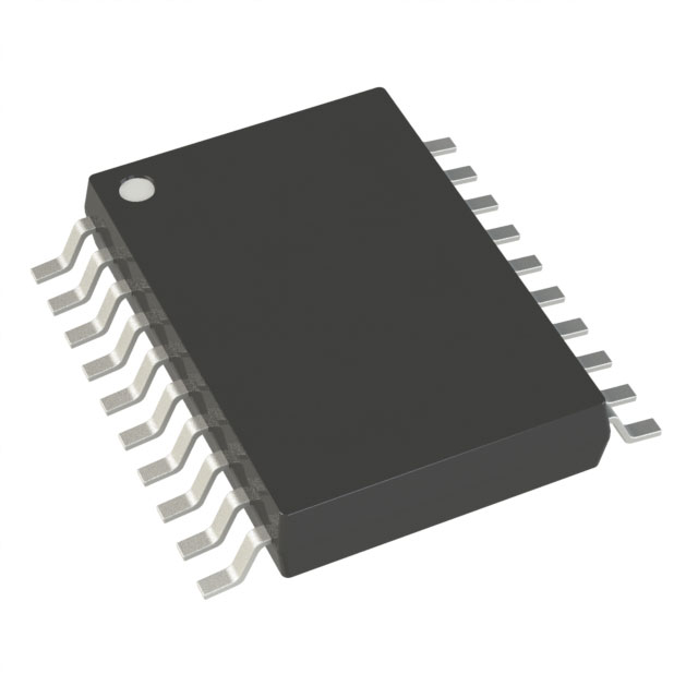
| Package / Case | 20-TSSOP |
| Package / Case [x] | 0.173 in |
| Package / Case [y] | 4.4 mm |
| Ratio - S/H:ADC | 1:1 |
| Reference Type | External, Internal |
| Sampling Rate (Per Second) | 1 M |
| Supplier Device Package | 20-TSSOP |
| Voltage - Supply, Analog [Max] | 5.25 V |
| Voltage - Supply, Analog [Min] | 2.7 V |
| Voltage - Supply, Digital [Max] | 5.25 V |
| Voltage - Supply, Digital [Min] | 2.7 V |
Pricing
Prices provided here are for design reference only. For realtime values and availability, please visit the distributors directly
| Distributor | Package | Quantity | $ | |
|---|---|---|---|---|
Description
General part information
AD7866 Series
The AD7866 is a dual 12-bit high-speed, low power, successive-approximation ADC. The part operates from a single 2.7 V to 5.25 V power supply and features throughput rates up to 1 MSPS. The device contains two ADCs, each preceded by a low-noise, wide bandwidth track/hold amplifier, which can handle input frequencies in excess of 10 MHz.The conversion process and data acquisition are controlled using standard control inputs allowing easy interfacing to microprocessors or DSPs. The input signal is sampled on the falling edge ofCSand conversion is also initiated at this point. The conversion time is determined by the SCLK frequency. There are no pipelined delays with the part.The AD7866 uses advanced design techniques to achieve very low power dissipation at high throughput rates. With 3 V supplies and 1 MSPS throughput rate, the part consumes a maximum of 3.8 mA. With 5 V supplies and 1 MSPS, the current consumption is a maximum of 4.8 mA. The part also offers flexible power/throughput rate management when operating in sleep mode.The analog input range for the part can be selected to be a 0 V to VREFrange or a 2 × VREFrange with either straight binary or twos complement output coding. The AD7866 has an on-chip 2.5 V reference that can be overdriven if an external reference is preferred. Each on-board ADC can also be supplied with a separate individual external reference.The AD7866 is available in a 20-lead thin shrink small outline (TSSOP) package.PRODUCT HIGHLIGHTSThe AD7866 features two complete ADC functions, allowing simultaneous sampling and conversion of two channels. Each ADC has a 2-channel input multiplexer. The conversion result of both channels is available simultaneously on separate data lines, or may be taken on one data line if only one serial port is available.High Throughput with Low Power Consumption—The AD7866 offers a 1 MSPS throughput rate with 11.4 mW maximum power consumption when operating at 3 V.Flexible Power/Throughput Rate Management—The conversion rate is determined by the serial clock, allowing the power consumption to be reduced as the conversion time is reduced through a SCLK frequency increase. Power efficiency can be maximized at lower throughput rates if the part enters sleep during conversions.No Pipeline Delay—The part features two standard successive approximation ADCs with accurate control of the sampling instant via aCSinput and once off conversion control.
Documents
Technical documentation and resources


