Deep-Dive with AI
Search across all available documentation for this part.

Deep-Dive with AI
Technical Specifications
Parameters and characteristics for this part
| Specification | ATXMEGA16A4U-CN |
|---|---|
| Connectivity | USB, UART/USART, SPI, IrDA, I2C |
| Core Processor | AVR |
| Core Size | 8 Bit, 16 Bit |
| Data Converters [custom] | 12 b |
| Data Converters [custom] | 12, 2 channels |
| Mounting Type | Surface Mount |
| Number of I/O | 34 |
| Operating Temperature [Max] | 105 °C |
| Operating Temperature [Min] | 0 °C |
| Oscillator Type | Internal |
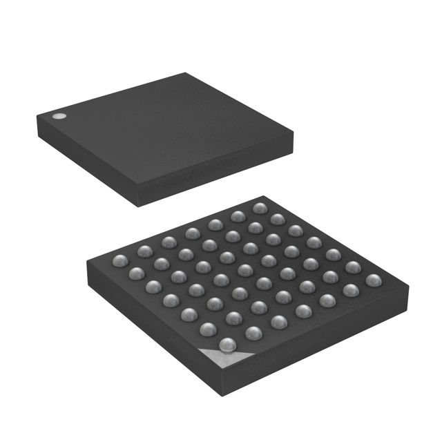
| Package / Case | 49-VFBGA |
| Peripherals | Brown-out Detect/Reset, DMA, POR, WDT, PWM |
| Program Memory Size | 16 KB |
| Program Memory Type | FLASH |
| RAM Size | 2K x 8 |
| Speed | 32 MHz |
| Supplier Device Package | 49-VFBGA (5x5) |
| Voltage - Supply (Vcc/Vdd) [Max] | 3.6 V |
| Voltage - Supply (Vcc/Vdd) [Min] | 1.6 V |
Pricing
Prices provided here are for design reference only. For realtime values and availability, please visit the distributors directly
| Distributor | Package | Quantity | $ | |
|---|---|---|---|---|
Description
General part information
ATxmega16A4U Series
The high-performance, low-power 8/16-bit AVR® XMEGA microcontroller combines 16KB ISP flash memory (plus 4KB boot code section) with read-while-write capabilities, 512B EEPROM, 2KB SRAM, eight-channel event system, a programmable multi-level interrupt controller, 26 general purpose I/O lines, one 16-bit real time counter, three flexible 16-bit timer/counters with compare modes and PWM, two USARTs (with SPI Master mode), one Two-Wire Interfaces (TWI) with SMBUs Level 1 support, one Serial Peripheral Interface (SPI), one 16-channel/12-bit 300 ksps A/D converter with optional differential input with programmable gain, one two-channel 12-bit 1 Msps D/A converter, two analog comparators with window mode, a programmable watchdog timer with separate internal oscillator, accurate internal oscillators with PLL and prescaler, and programmable brown-out detection.
The XMEGA E devices feature an innovative XMEGA Custom Logic module (XCL) consisting of two independent 8-bit timer/counters and two lookup tables used for defining glue logic. It is designed to reduce bill of material (BOM) and PCB size as the XCL can replace external circuitry such as delay elements, RS-latches, D-latches, D-flip-flops chip-select logic, AND, NAND, OR, NOR, XOR, XNOR, NOT, MUX AND/OR/XOR logic gates. In addition it can together with the USART enable customized communication protocols. By executing powerful instructions in a single clock cycle, the device achieves throughputs approaching 1 MIPS per MHz, balancing power consumption and processing speed.
Documents
Technical documentation and resources


