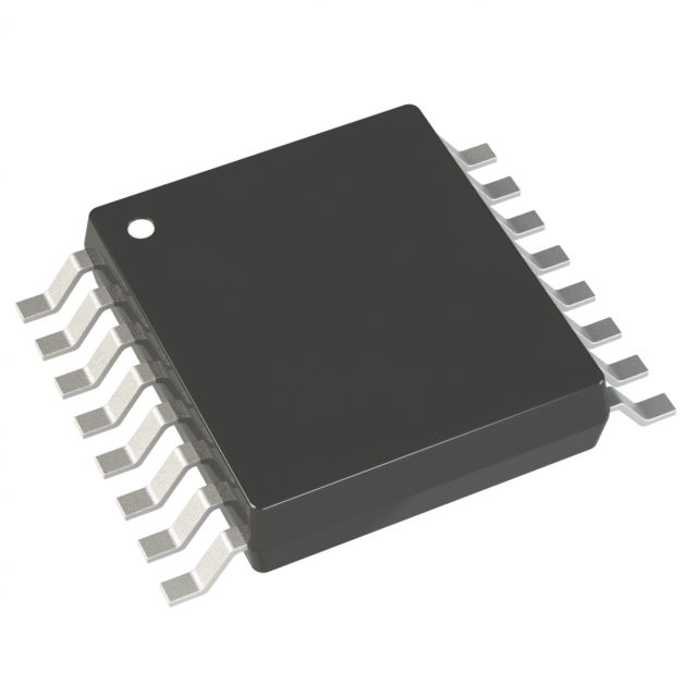
ADG1609BRUZ-REEL7
Active4.5 Ω RON, 4-CHANNEL ±5 V,+12 V, +5 V, AND +3.3 V MULTIPLEXER
Deep-Dive with AI
Search across all available documentation for this part.

ADG1609BRUZ-REEL7
Active4.5 Ω RON, 4-CHANNEL ±5 V,+12 V, +5 V, AND +3.3 V MULTIPLEXER
Deep-Dive with AI
Technical Specifications
Parameters and characteristics for this part
| Specification | ADG1609BRUZ-REEL7 |
|---|---|
| -3db Bandwidth | 78 MHz |
| Channel Capacitance (CS(off), CD(off)) [custom] | 59 pF |
| Channel Capacitance (CS(off), CD(off)) [custom] | 19 pF |
| Channel-to-Channel Matching (ΔRon) | 120 mOhm |
| Charge Injection | 29 pC |
| Crosstalk | -64 dB |
| Current - Leakage (IS(off)) (Max) | 100 pA |
| Mounting Type | Surface Mount |
| Multiplexer/Demultiplexer Circuit | 4:1 |
| Number of Circuits | 2 |
| On-State Resistance (Max) [Max] | 4.5 Ohm |
| Operating Temperature [Max] | 125 °C |
| Operating Temperature [Min] | -40 °C |
| Package / Case | 16-TSSOP |
| Package / Case [x] | 0.173 in |
| Package / Case [y] | 4.4 mm |
| Supplier Device Package | 16-TSSOP |
| Switch Circuit | SP4T |
| Switch Time (Ton, Toff) (Max) [custom] | 94 ns |
| Switch Time (Ton, Toff) (Max) [custom] | 93 ns |
| Voltage - Supply, Dual (V±) | 8 V, 3.3 V |
| Voltage - Supply, Single (V+) [Max] | 16 V |
| Voltage - Supply, Single (V+) [Min] | 3.3 V |
Pricing
Prices provided here are for design reference only. For realtime values and availability, please visit the distributors directly
| Distributor | Package | Quantity | $ | |
|---|---|---|---|---|
| Digikey | Cut Tape (CT) | 1 | $ 13.03 | |
| 10 | $ 9.21 | |||
| 25 | $ 8.23 | |||
| 100 | $ 7.13 | |||
| 250 | $ 6.60 | |||
| 500 | $ 6.27 | |||
| Digi-Reel® | 1 | $ 13.03 | ||
| 10 | $ 9.21 | |||
| 25 | $ 8.23 | |||
| 100 | $ 7.13 | |||
| 250 | $ 6.60 | |||
| 500 | $ 6.27 | |||
| Tape & Reel (TR) | 1000 | $ 6.06 | ||
Description
General part information
ADG1609 Series
TheADG1608/ ADG1609 are monolithic CMOS analog multiplexers comprising eight single channels and four differential channels, respectively. The ADG1608 switches one of eight inputs to a common output, as determined by the 3-bit binary address lines, A0, A1, and A2. The ADG1609 switches one of four differential inputs to a common differential output, as determined by the 2-bit binary address lines, A0 and A1. An EN input on both devices is used to enable or disable the device. When disabled, all channels are switched off.Each switch conducts equally well in both directions when on and has an input signal range that extends to the supplies. In the off condition, signal levels up to the supplies are blocked. All switches exhibit break-before-make switching action. Inherent in the design is low charge injection for minimum transients when switching the digital inputs.The low on resistance of these switches make them ideal solutions for data acquisition and gain switching applications where low on resistance and distortion is critical. The on-resistance profile is very flat over the full analog input range, ensuring excellent linearity and low distortion when switching audio signals.CMOS construction ensures ultralow power dissipation, making the parts ideally suited for portable and battery-powered instruments.APPLICATIONSCommunication systemsMedical systemsAudio signal routingVideo signal routingAutomatic test equipmentData acquisition systemsBattery-powered systemsSample-and-hold systemsRelay replacements
Documents
Technical documentation and resources


