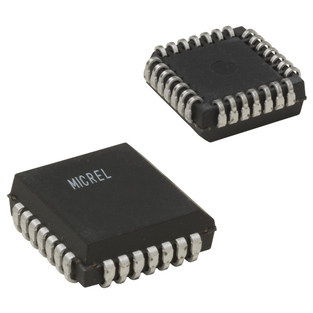
MIC5801BV
ObsoleteLATCH BASED PERIPHERAL DRIVER 8 DRIVER BIMOS PQCC28
Deep-Dive with AI
Search across all available documentation for this part.

MIC5801BV
ObsoleteLATCH BASED PERIPHERAL DRIVER 8 DRIVER BIMOS PQCC28
Deep-Dive with AI
Technical Specifications
Parameters and characteristics for this part
| Specification | MIC5801BV |
|---|---|
| Current - Output (Max) [Max] | 500 mA |
| Interface | Parallel, Strobe |
| Mounting Type | Surface Mount |
| Number of Outputs | 8 |
| Operating Temperature [Max] | 85 °C |
| Operating Temperature [Min] | -40 °C |
| Output Configuration | Low Side |
| Output Type | Bipolar |
| Package / Case | 28-LCC (J-Lead) |
| Ratio - Input:Output [custom] | 1:1 |
| Supplier Device Package | 28-PLCC (11.48x11.48) |
| Switch Type | Latched Driver |
| Voltage - Load [Max] | 50 V |
Pricing
Prices provided here are for design reference only. For realtime values and availability, please visit the distributors directly
| Distributor | Package | Quantity | $ | |
|---|---|---|---|---|
Description
General part information
MIC5801 Series
The MIC5800/5801 latched drivers are high-voltage, high-current integrated circuits comprised of four or eight CMOS data latches, a bipolar Darlington transistor driver for each latch, and CMOS control circuitry for the common CLEAR, STROBE, and OUTPUT ENABLE functions.
The bipolar/MOS combination provides an extremely low-power latch with maximum interface flexibility. MIC5800 contains four latched drivers; MIC5801 contains eight latched drivers.
Data input rates are greatly improved in these devices. With a 5V supply, they will typically operate at better than 5MHz. With a 12V supply, significantly higher speeds are obtained. The CMOS inputs are compatible with standard CMOS, PMOS, and NMOS circuits. TTL or DTL circuits may require the use of appropriate pull-up resistors. The bipolar outputs are suitable for use with relays, solenoids, stepping motors, LED or incandescent displays, and other high-power loads. Both units have open-collector outputs and integral diodes for inductive load transient suppression. The output transistors are capable of sinking 500mA and will sustain at least 50V in the OFF state. Because of limitations on package power dissipation, the simultaneous operation of all drivers at maximum rated current can only be accomplished by a reduction in duty cycle. Outputs may be paralleled for higher load current capability.
Documents
Technical documentation and resources


