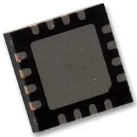
AD5592RWBCPZ-RL7
ActiveADC / DAC IC, ON-CHIP REFERENCE, CONFIGURABLE, 2.7 V TO 5.5 V IN, LFCSP-16, -40 °C TO 125 °C
Deep-Dive with AI
Search across all available documentation for this part.

AD5592RWBCPZ-RL7
ActiveADC / DAC IC, ON-CHIP REFERENCE, CONFIGURABLE, 2.7 V TO 5.5 V IN, LFCSP-16, -40 °C TO 125 °C
Technical Specifications
Parameters and characteristics for this part
| Specification | AD5592RWBCPZ-RL7 |
|---|---|
| Data Interface | SPI |
| Grade | Automotive |
| Mounting Type | Surface Mount |
| Number of Channels | 8 |
| Operating Temperature [Max] | 125 °C |
| Operating Temperature [Min] | -40 °C |
| Package / Case | 16-WFQFN, CSP |
| Qualification | AEC-Q100 |
| Resolution (Bits) | 12 b |
| Sampling Rate (Per Second) | 350 kPer Second |
| Supplier Device Package | 16-LFCSP-WQ (3x3) |
| Type | DAC, ADC |
| Voltage Supply Source | Single Supply |
Pricing
Prices provided here are for design reference only. For realtime values and availability, please visit the distributors directly
Description
General part information
AD5592R Series
The AD5592R/AD5592R-1 have eight I/Ox pins (I/O0 to I/O7) that can be independently configured as digital-to-analog converter (DAC) outputs, analog-to-digital converter (ADC) inputs, digital outputs, or digital inputs. When an I/Ox pin is configured as an analog output, it is driven by a 12-bit DAC. The output range of the DAC is 0 V to VREFor 0 V to 2 × VREF. When an I/Ox pin is configured as an analog input, it is connected to a 12-bit ADC via an analog multiplexer. The input range of the ADC is 0 V to VREFor 0 V to 2 × VREF. The ADC has a total throughput rate of 400 kSPS. The I/Ox pins can also be configured as digital, general-purpose input or output (GPIO) pins. The state of the GPIO pins can be set or read back by accessing the GPIO write data register or the GPIO read configuration register, respectively, via a serial peripheral interface (SPI) write or read operation.The AD5592R/AD5592R-1 have an integrated 2.5 V, 20 ppm/°C reference, which is turned off by default, and an integrated temperature indicator, which gives an indication of the die temperature. The temperature value is read back as part of an ADC read sequence.The AD5592R/AD5592R-1 are available in 16-ball, 2 mm × 2 mm WLCSP, 16-lead, 3 mm × 3 mm LFCSP, and 16-lead TSSOP. The AD5592R/AD5592R-1 operate over a temperature range of −40 °C (TA) to +125 °C (TJ).APPLICATIONSControl and monitoringGeneral-purpose analog and digital inputs/outputs
Documents
Technical documentation and resources


