Deep-Dive with AI
Search across all available documentation for this part.

Deep-Dive with AI
Technical Specifications
Parameters and characteristics for this part
| Specification | CD4006BF3A |
|---|---|
| Logic Type | Shift Register |
| Mounting Type | Through Hole |
| Number of Bits per Element | 18 |
| Number of Elements | 1 |
| Operating Temperature [Max] | 125 °C |
| Operating Temperature [Min] | -55 °C |
| Output Type | Non-Inverted |
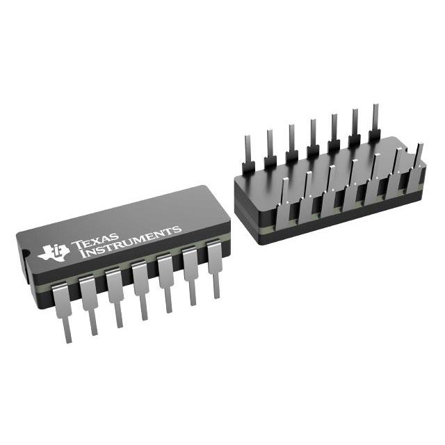
| Package / Case | 14-CDIP |
| Supplier Device Package | 14-CDIP |
| Voltage - Supply [Max] | 18 V |
| Voltage - Supply [Min] | 3 V |
Pricing
Prices provided here are for design reference only. For realtime values and availability, please visit the distributors directly
| Distributor | Package | Quantity | $ | |
|---|---|---|---|---|
| Texas Instruments | TUBE | 1 | $ 22.72 | |
| 100 | $ 19.85 | |||
| 250 | $ 15.30 | |||
| 1000 | $ 13.69 | |||
Description
General part information
CD4006B-MIL Series
CD4006B types are composed of 4 separate shift register sections: two sections of four stages and two sections of five stages with an output tap at the fourth stage. Each section has an independent single-rail data path.
A common clock signal is used for all stages. Data are shifted to the next stage on negative-going transitions of the clock. Through appropriate connections of inputs and outputs, multiple register sections of 4, 5, 8, and 9 stages or single register sections of 10, 12, 13, 14, 16, 17 and 18 stages can be implemented using one CD4006B package. Longer shift register sections can be assembled by using more than one CD4006B.
To facilitate cascading stages when clock rise and fall times are slow, an optional output (D1+4') that is delayed one-half clock-cycle, is provided (see Truth Table for Output from Term. 2).
Documents
Technical documentation and resources


