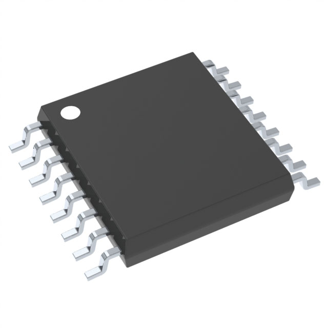
DS90CR286ATDGGQ1
Active3.3 V RISING EDGE DATA STROBE LVDS RECEIVER 28-BIT CHAN LINK 66 MHZ
Deep-Dive with AI
Search across all available documentation for this part.

DS90CR286ATDGGQ1
Active3.3 V RISING EDGE DATA STROBE LVDS RECEIVER 28-BIT CHAN LINK 66 MHZ
Technical Specifications
Parameters and characteristics for this part
| Specification | DS90CR286ATDGGQ1 |
|---|---|
| Grade | Automotive |
| Mounting Type | Surface Mount |
| Package / Case | 16-TSSOP |
| Package / Case [x] | 0.173 in |
| Package / Case [y] | 4.4 mm |
| Qualification | AEC-Q100 |
| Supplier Device Package | 16-TSSOP |
| Voltage - Supply [Max] | 3.6 V |
| Voltage - Supply [Min] | 3 V |
Pricing
Prices provided here are for design reference only. For realtime values and availability, please visit the distributors directly
| Distributor | Package | Quantity | $ | |
|---|---|---|---|---|
| Digikey | Tube | 102 | $ 9.04 | |
| Texas Instruments | TUBE | 1 | $ 9.12 | |
| 100 | $ 7.96 | |||
| 250 | $ 6.14 | |||
| 1000 | $ 5.49 | |||
Description
General part information
DS90CR286AT-Q1 Series
The DS90CR286AT-Q1 receiver converts four LVDS (Low Voltage Differential Signaling) data streams back into parallel 28 bits of LVCMOS data. The receiver data outputs strobe on the output clock's rising edge.
The receiver LVDS clock operates at rates from 20 to 66 MHz. The DS90CR286AT-Q1 phase-locks to the input LVDS clock, samples the serial bit streams at the LVDS data lines, and converts them into 28-bit parallel output data. At an incoming clock rate of 66 MHz, each LVDS input line is running at a bit rate of 462 Mbps, resulting in a maximum throughput of 1.848 Gbps.
The DS90CR286AT-Q1 device is enhanced over prior generation receivers due to a wider data valid time on the receiver output. The DS90CR286AT-Q1 is designed for PCB board chip-to-chip OpenLDI-to-RGB bridge conversion. LVDS data transmission over cable interconnect is not recommended for this device.
Documents
Technical documentation and resources


