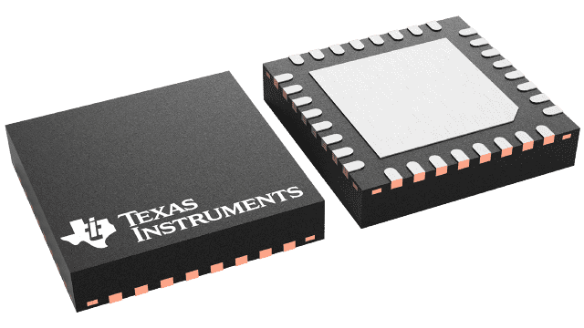
CDCM9102RHBT
ActiveLOW NOISE TWO CHANNEL 100-MHZ PCIE CLOCK GENERATOR
Deep-Dive with AI
Search across all available documentation for this part.

CDCM9102RHBT
ActiveLOW NOISE TWO CHANNEL 100-MHZ PCIE CLOCK GENERATOR
Deep-Dive with AI
Technical Specifications
Parameters and characteristics for this part
| Specification | CDCM9102RHBT |
|---|---|
| Differential - Input:Output | No/Yes |
| Divider/Multiplier | False |
| Input | Crystal |
| Mounting Type | Surface Mount |
| Number of Circuits | 1 |
| Operating Temperature [Max] | 85 °C |
| Operating Temperature [Min] | -40 °C |
| Output | LVDS, LVPECL, LVCMOS |
| Package / Case | 32-VFQFN Exposed Pad |
| PLL | False |
| Ratio - Input:Output [custom] | 1:3 |
| Supplier Device Package | 32-VQFN (5x5) |
| Type | Clock Generator |
| Voltage - Supply [Max] | 3.6 V |
| Voltage - Supply [Min] | 3 V |
Pricing
Prices provided here are for design reference only. For realtime values and availability, please visit the distributors directly
| Distributor | Package | Quantity | $ | |
|---|---|---|---|---|
| Digikey | Cut Tape (CT) | 1 | $ 4.21 | |
| 10 | $ 3.78 | |||
| 25 | $ 3.58 | |||
| 100 | $ 3.10 | |||
| Digi-Reel® | 1 | $ 4.21 | ||
| 10 | $ 3.78 | |||
| 25 | $ 3.58 | |||
| 100 | $ 3.10 | |||
| Tape & Reel (TR) | 250 | $ 2.94 | ||
| 500 | $ 2.80 | |||
| Texas Instruments | SMALL T&R | 1 | $ 4.12 | |
| 100 | $ 3.36 | |||
| 250 | $ 2.64 | |||
| 1000 | $ 2.24 | |||
Description
General part information
CDCM9102 Series
The CDCM9102 is a low-jitter clock generator designed to provide reference clocks for communications standards such as PCI Express™. The device supports up to PCIE gen3 and is easy to configure and use. The CDCM9102 provides two 100-MHz differential clock ports. The output types supported for these ports include LVPECL, LVDS, or a pair of LVCMOS buffers. HCSL signaling is supported using an AC-coupled network. The user configures the output buffer type desired by strapping device pins. Additionally, a single-ended 25-MHz clock output port is provided. Uses for this port include general-purpose clocking, clocking Ethernet PHYs, or providing a reference clock for additional clock generators. All clocks generated are derived from a single external 25-MHz crystal.
The CDCM9102 is a low-jitter clock generator designed to provide reference clocks for communications standards such as PCI Express™. The device supports up to PCIE gen3 and is easy to configure and use. The CDCM9102 provides two 100-MHz differential clock ports. The output types supported for these ports include LVPECL, LVDS, or a pair of LVCMOS buffers. HCSL signaling is supported using an AC-coupled network. The user configures the output buffer type desired by strapping device pins. Additionally, a single-ended 25-MHz clock output port is provided. Uses for this port include general-purpose clocking, clocking Ethernet PHYs, or providing a reference clock for additional clock generators. All clocks generated are derived from a single external 25-MHz crystal.
Documents
Technical documentation and resources


