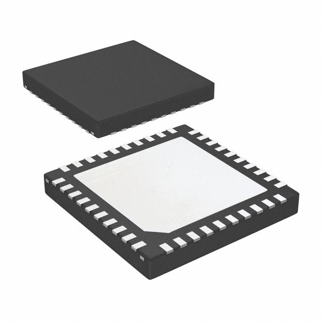
DS25BR440TSQX/NOPB
Active3.125-GBPS QUAD LVDS BUFFER WITH TRANSMIT PRE-EMPHASIS AND RECEIVE EQUALIZATION
Deep-Dive with AI
Search across all available documentation for this part.

DS25BR440TSQX/NOPB
Active3.125-GBPS QUAD LVDS BUFFER WITH TRANSMIT PRE-EMPHASIS AND RECEIVE EQUALIZATION
Deep-Dive with AI
Technical Specifications
Parameters and characteristics for this part
| Specification | DS25BR440TSQX/NOPB |
|---|---|
| Applications | LVDS |
| Current - Supply | 162 mA |
| Delay Time | 400 ps |
| Mounting Type | Surface Mount |
| Number of Channels | 4 |
| Operating Temperature [Max] | 85 °C |
| Operating Temperature [Min] | -40 °C |
| Output | LVDS |
| Package / Case | 40-WFQFN Exposed Pad |
| Signal Conditioning | Output Pre-Emphasis, Input Equalization |
| Supplier Device Package | 40-WQFN (6x6) |
| Type | ReDriver, Buffer |
| Voltage - Supply [Max] | 3.6 V |
| Voltage - Supply [Min] | 3 V |
Pricing
Prices provided here are for design reference only. For realtime values and availability, please visit the distributors directly
| Distributor | Package | Quantity | $ | |
|---|---|---|---|---|
| Digikey | Cut Tape (CT) | 1 | $ 7.53 | |
| Digi-Reel® | 1 | $ 7.53 | ||
| Tape & Reel (TR) | 2500 | $ 4.11 | ||
| Texas Instruments | LARGE T&R | 1 | $ 5.76 | |
| 100 | $ 4.70 | |||
| 250 | $ 3.69 | |||
| 1000 | $ 3.13 | |||
Description
General part information
DS25BR440 Series
The DS25BR440 is a 3.125 Gbps Quad LVDS buffer optimized for high-speed signal routing and repeating over lossy FR-4 printed circuit board backplanes and balanced cables. Fully differential signal paths ensure exceptional signal integrity and noise immunity.
The DS25BR440 features two levels of transmit pre-emphasis (PE) and two levels of receive equalization (EQ). Both of these features compensate for interconnect losses and ultimately maximize noise margin. A loss-of-signal (LOS) circuit monitors each input channel and a uniqueLOSpin is asserted when no signal is detected at that input.
Wide input common mode range allows the switch to accept signals with LVDS, CML and LVPECL levels; the output levels are LVDS. A very small package footprint requires a minimal space on the board while the flow-through pinout allows easy board layout. Each differential input and output is internally terminated with a 100Ω resistor to lower device return losses, reduce component count and further minimize board space.
Documents
Technical documentation and resources


