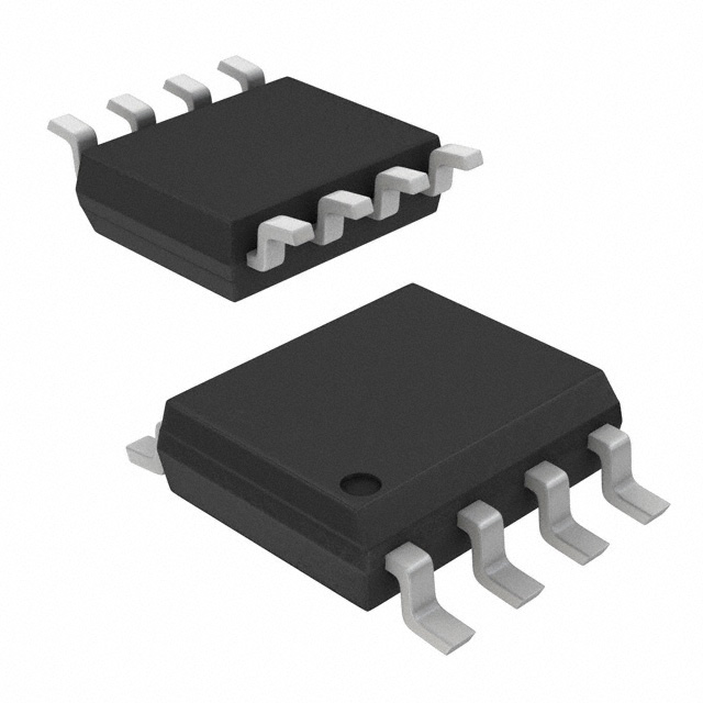
FQS4900TF
ActiveTRANSISTOR,MOSFET,PAIR,COMPLEMENTARY,60V V(BR)DSS,1.3A I(D),SO ROHS COMPLIANT: YES
Deep-Dive with AI
Search across all available documentation for this part.

FQS4900TF
ActiveTRANSISTOR,MOSFET,PAIR,COMPLEMENTARY,60V V(BR)DSS,1.3A I(D),SO ROHS COMPLIANT: YES
Deep-Dive with AI
Technical Specifications
Parameters and characteristics for this part
| Specification | FQS4900TF |
|---|---|
| Configuration | N and P-Channel |
| Current - Continuous Drain (Id) @ 25°C | 1.3 A, 300 mA |
| Drain to Source Voltage (Vdss) | 300 V, 60 V |
| Gate Charge (Qg) (Max) @ Vgs | 2.1 nC |
| Mounting Type | Surface Mount |
| Operating Temperature [Max] | 150 °C |
| Operating Temperature [Min] | -55 °C |
| Package / Case | 8-SOIC |
| Package / Case [x] | 0.154 in |
| Package / Case [y] | 3.9 mm |
| Power - Max [Max] | 2 W |
| Rds On (Max) @ Id, Vgs | 550 mOhm |
| Supplier Device Package | 8-SOIC |
| Technology | MOSFET (Metal Oxide) |
| Vgs(th) (Max) @ Id | 1.95 V |
Pricing
Prices provided here are for design reference only. For realtime values and availability, please visit the distributors directly
| Distributor | Package | Quantity | $ | |
|---|---|---|---|---|
| Digikey | Bulk | 517 | $ 0.58 | |
Description
General part information
FQS4900 Series
These dual N and P-channel enhancement mode power field effect transistors are produced using ON Semiconductor's proprietary, planar stripe, DMOS technology.This advanced technology has been especially tailored to minimize on-state resistance, provide superior switching performance, and withstand high energy pulse in the avalanche and communication mode. This device is well suited for high interface in telephone sets.
Documents
Technical documentation and resources


