Deep-Dive with AI
Search across all available documentation for this part.

Deep-Dive with AI
Technical Specifications
Parameters and characteristics for this part
| Specification | AD8338ACPZ-R7 |
|---|---|
| -3db Bandwidth | 18 MHz |
| Mounting Type | Surface Mount |
| Number of Circuits | 1 |
| Operating Temperature [Max] | 85 °C |
| Operating Temperature [Min] | -40 °C |
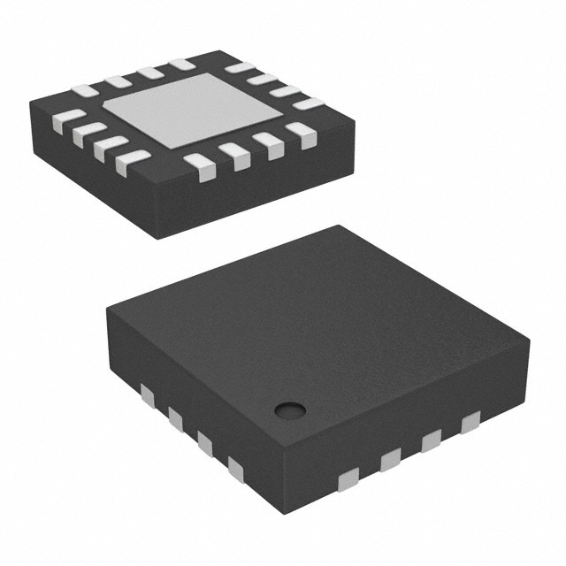
| Package / Case | 16-WFQFN Exposed Pad, CSP |
| Slew Rate | 50 V/µs |
| Supplier Device Package | 16-LFCSP (3x3) |
| Voltage - Supply Span (Max) [Max] | 5 V |
| Voltage - Supply Span (Min) [Min] | 3 V |
Pricing
Prices provided here are for design reference only. For realtime values and availability, please visit the distributors directly
| Distributor | Package | Quantity | $ | |
|---|---|---|---|---|
| Digikey | Cut Tape (CT) | 1 | $ 15.31 | |
| 10 | $ 10.93 | |||
| 25 | $ 9.81 | |||
| 100 | $ 8.55 | |||
| 250 | $ 7.94 | |||
| 500 | $ 7.57 | |||
| Digi-Reel® | 1 | $ 15.31 | ||
| 10 | $ 10.93 | |||
| 25 | $ 9.81 | |||
| 100 | $ 8.55 | |||
| 250 | $ 7.94 | |||
| 500 | $ 7.57 | |||
| Tape & Reel (TR) | 1500 | $ 7.45 | ||
Description
General part information
AD8338 Series
The AD8338 is a variable gain amplifier (VGA) for applications that require a fully differential signal path, low power, low noise, and a well-defined gain over frequency. Although the inputs are differential, the device can also be driven with a single-ended source if required.The basic gain function is linear-in-dB and is controlled by the voltage applied to Pin GAIN. The nominal gain range spans from 0 dB to 80 dB for control voltages between 0.1 V to 1.1 V with a slope of 12.5 mV/dB. The nominal gain range can be shifted up or down via direct access to Pin INPD and Pin INMD, the current inputs of the VGA. For example, driving the INPD and INMD pins with 50 Ω resistors shifts the gain range up by 20 dB, that is, 20 dB to 100 dB, and lowers the input referred noise of the device to 1.5 nV/√Hz. Additionally, the gain slope can be inverted via logic Pin MODE.The AD8338 includes additional circuit blocks to enable input offset correction and automatic gain control (AGC). DC offset voltages are removed by the offset correction circuit, which behaves like a high-pass filter whose corner is set with an external capacitor. The AGC function varies the gain of the AD8338 to maintain a constant rms output voltage. An externally applied voltage to Pin VAGC with respect to the voltage at Pin VREF sets the output rms amplitude. A capacitor from Pin DETO to ground sets the response time of the AGC circuit.The AD8338 offers additional versatility by providing access to the internal summing nodes of the VGA core and the output amplifiers. With the addition of a few external passive components, users can customize the gain, bandwidth, input impedance, and noise profile of the device to fit their application.The AD8338 uses a single-supply voltage of 3.0 V to 5.0 V and is very power efficient, consuming as little as 3 mA quiescent current at mid gain. The AD8338 is available in a 3 mm × 3 mm, RoHS-compliant, 16-lead LFCSP and is specified over the industrial temperature range of −40°C to +85°C.APPLICATIONSFront end for inductive telemetry systemsUltrasonic signal receiversSignal compression for driving an ADCAGC amplifiers


