Deep-Dive with AI
Search across all available documentation for this part.

Deep-Dive with AI
Technical Specifications
Parameters and characteristics for this part
| Specification | AD603AR-REEL7 |
|---|---|
| -3db Bandwidth | 90 MHz |
| Current - Input Bias | 200 nA |
| Current - Output / Channel | 50 mA |
| Current - Supply | 12.5 mA |
| Mounting Type | Surface Mount |
| Number of Circuits | 1 |
| Operating Temperature [Max] | 85 °C |
| Operating Temperature [Min] | -40 °C |
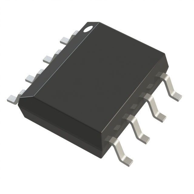
| Package / Case | 8-SOIC |
| Package / Case [x] | 0.154 in |
| Package / Case [y] | 3.9 mm |
| Slew Rate | 275 V/µs |
| Supplier Device Package | 8-SOIC |
| Voltage - Supply Span (Max) [Max] | 12.6 V |
| Voltage - Supply Span (Min) [Min] | 9.5 V |
Pricing
Prices provided here are for design reference only. For realtime values and availability, please visit the distributors directly
| Distributor | Package | Quantity | $ | |
|---|---|---|---|---|
Description
General part information
AD603 Series
The AD603 is a low noise, voltage-controlled amplifier for use in RF and IF AGC systems. It provides accurate, pin-selectable gains of −11 dB to +31 dB with a bandwidth of 90 MHz or +9 dB to 51+ dB with a bandwidth of 9 MHz. Any intermediate gain range may be arranged using one external resistor. The input referred noise spectral density is only 1.3 nV/√Hz, and power consumption is 125 mW at the recommended ±5 V supplies.The decibel gain is linear in dB, accurately calibrated, and stable over temperature and supply. The gain is controlled at a high impedance (50 MΩ), low bias (200 nA) differential input; the scaling is 25 mV/dB, requiring a gain control voltage of only 1 V to span the central 40 dB of the gain range. An overrange and underrange of 1 dB is provided whatever the selected range. The gain control response time is less than 1 μs for a 40 dB change.The differential gain control interface allows the use of either differential or single-ended positive or negative control voltages. Several of these amplifiers may be cascaded and their gain control gains offset to optimize the system SNR.The AD603 can drive a load impedance as low as 100 Ω with low distortion. For a 500 Ω load in shunt with 5 pF, the total harmonic distortion for a ±1 V sinusoidal output at 10 MHz is typically −60 dBc. The peak specified output is ±2.5 V minimum into a 500 Ω load.The AD603 uses a patented proprietary circuit topology—the X-AMP®. The X-AMP comprises a variable attenuator of 0 dB to −42.14 dB followed by a fixed-gain amplifier. Because of the attenuator, the amplifier never has to cope with large inputs and can use negative feedback to define its (fixed) gain and dynamic performance. The attenuator has an input resistance of 100 Ω, laser trimmed to ±3%, and comprises a 7-stage R-2R ladder network, resulting in an attenuation between tap points of 6.021 dB. A proprietary interpolation technique provides a continuous gain control function that is linear in dB.The AD603 is specified for operation from −40°C to +85°C.ApplicationsRF/IF AGC amplifiersVideo gain controlsA/D range extensionsSignal measurements
Documents
Technical documentation and resources


