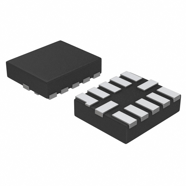
NLSX4014MUTAG
Obsolete4-BIT 100 MBPS CONFIGURABLE DUAL-SUPPLY LEVEL TRANSLATOR
Deep-Dive with AI
Search across all available documentation for this part.

NLSX4014MUTAG
Obsolete4-BIT 100 MBPS CONFIGURABLE DUAL-SUPPLY LEVEL TRANSLATOR
Deep-Dive with AI
Technical Specifications
Parameters and characteristics for this part
| Specification | NLSX4014MUTAG |
|---|---|
| Channel Type | Bidirectional |
| Channels per Circuit | 4 |
| Data Rate | 140 Mbps |
| Features | Auto-Direction Sensing |
| Mounting Type | Surface Mount |
| Number of Circuits | 1 |
| Operating Temperature [Max] | 85 °C |
| Operating Temperature [Min] | -40 °C |
| Output Type | Tri-State, Non-Inverted |
| Package / Case | 12-UFQFN |
| Supplier Device Package | 12-UQFN |
| Supplier Device Package [x] | 1.7 |
| Supplier Device Package [y] | 2 |
| Translator Type | Voltage Level |
| Voltage - VCCA [Max] | 4.1 V |
| Voltage - VCCA [Min] | 0.9 V |
| Voltage - VCCB [Max] | 4.5 V |
| Voltage - VCCB [Min] | 1.3 V |
Pricing
Prices provided here are for design reference only. For realtime values and availability, please visit the distributors directly
| Distributor | Package | Quantity | $ | |
|---|---|---|---|---|
| Digikey | Cut Tape (CT) | 1 | $ 1.86 | |
| 10 | $ 1.14 | |||
| 25 | $ 0.96 | |||
| 100 | $ 0.77 | |||
| 250 | $ 0.68 | |||
| 500 | $ 0.62 | |||
| 1000 | $ 0.57 | |||
| Digi-Reel® | 1 | $ 1.86 | ||
| 10 | $ 1.14 | |||
| 25 | $ 0.96 | |||
| 100 | $ 0.77 | |||
| 250 | $ 0.68 | |||
| 500 | $ 0.62 | |||
| 1000 | $ 0.57 | |||
| Tape & Reel (TR) | 3000 | $ 0.50 | ||
| 6000 | $ 0.48 | |||
| 15000 | $ 0.47 | |||
Description
General part information
NLSX4014 Series
The NLSX4014 is a 4 bit configurable dual supply bidirectional level translator without a direction control pin. The I/O VCC- and I/O VLports are designed to track two different power supply rails, VCCand VLrespectively. The VCCsupply rail is configurable from 1.3 V to 4.5 V while the VL supply rail is configurable from 0.9 V to (VCC- 0.4) V. This allows lower voltage logic signals on the VL side to be translated into higher voltage logic signals on the VCCside, and vice versa. Both I/O ports are auto sensing; thus, no direction pin is required.The Output Enable (EN) input, when Low, disables both I/O ports by putting them in 3 state. This significantly reduces the supply currents from both VCCand VL. The EN signal is designed to track VL.
Documents
Technical documentation and resources


