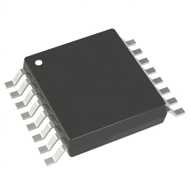
AD5668BRUZ-3REEL7
ActiveOCTAL, 16-BIT, SPI VOLTAGE OUTPUTDENSEDAC WITH 5 PPM/°C ON-CHIP REFERENCE
Deep-Dive with AI
Search across all available documentation for this part.

AD5668BRUZ-3REEL7
ActiveOCTAL, 16-BIT, SPI VOLTAGE OUTPUTDENSEDAC WITH 5 PPM/°C ON-CHIP REFERENCE
Technical Specifications
Parameters and characteristics for this part
| Specification | AD5668BRUZ-3REEL7 |
|---|---|
| Architecture | String DAC |
| Data Interface | DSP, SPI |
| Differential Output | False |
| INL/DNL (LSB) | 8 LSB, 1 LSB |
| Mounting Type | Surface Mount |
| Number of Bits | 16 |
| Number of D/A Converters | 8 |
| Operating Temperature [Max] | 105 ░C |
| Operating Temperature [Min] | -40 °C |
| Output Type | Voltage - Buffered |
| Package / Case | 16-TSSOP |
| Package / Case [x] | 0.173 in |
| Package / Case [y] | 4.4 mm |
| Reference Type | External, Internal |
| Settling Time | 7 µs |
| Supplier Device Package | 16-TSSOP |
| Voltage - Supply, Analog [Max] | 5.5 V |
| Voltage - Supply, Analog [Min] | 2.7 V |
| Voltage - Supply, Digital [Max] | 5.5 V |
| Voltage - Supply, Digital [Min] | 2.7 V |
Pricing
Prices provided here are for design reference only. For realtime values and availability, please visit the distributors directly
| Distributor | Package | Quantity | $ | |
|---|---|---|---|---|
| Digikey | Tape & Reel (TR) | 1000 | $ 20.23 | |
Description
General part information
AD5668 Series
The AD5668 device is a low power, octal, 16-bit, buffered voltage-output DAC. All devices operate from a single 2.7 V to 5.5 V supply and are guaranteed monotonic by design. The AD5668 and AD5628 are available in both a 4 mm × 4 mm LFCSP and a 16-lead TSSOP, while the AD5648 is available in both a 14-lead and 16-lead TSSOP.The AD5628/AD5648/AD5668 have an on-chip reference with an internal gain of 2. The AD5628-1/AD5648-1/AD5668-1 have a 1.25 V 5 ppm/°C reference, giving a full-scale output range of 2.5 V; the AD5628-2/AD5648-2/AD5668-2 and AD5668-3 have a 2.5 V 5 ppm/°C reference, giving a full-scale output range of 5 V. The on-board reference is off at power-up, allowing the use of an external reference. The internal reference is enabled via a software write.The part incorporates a power-on reset circuit that ensures that the DAC output powers up to 0 V (AD5628-1/AD5648-1/AD5668-1, AD5628-2/AD5648-2/AD5668-2) or midscale (AD5668-3) and remains powered up at this level until a valid write takes place. The part contains a power-down feature that reduces the current consumption of the device to 400 nA at 5 V and provides software-selectable output loads while in power-down mode for any or all DAC channels. The outputs of all DACs can be updated simultaneously using theLDACfunction, with the added functionality of user-selectableDACchannels to simultaneously update. There is also an asynchronous CLR that updates all DACs to a userprogrammable code—zero scale, midscale, or full scale.The AD5628/AD5648/AD5668 utilize a versatile 3-wire serial interface that operates at clock rates of up to 50 MHz and is compatible with standard SPI®, QSPI™, MICROWIRE™, and DSP interface standards. The on-chip precision output amplifier enables rail-to-rail output swing.Product HighlightsOctal, 12-/14-/16-bit DAC.On-chip 1.25 V/2.5 V, 5 ppm/°C reference.Available in 14-lead/16-lead TSSOP, 16-lead LFCSP, and 16-ball WLCSP.Power-on reset to 0 V or midscale.Power-down capability. When powered down, the DAC typically consumes 200 nA at 3 V and 400 nA at 5 V.ApplicationsProcess controlData acquisition systemsPortable battery-powered instrumentsDigital gain and offset adjustmentProgrammable voltage and current sourcesProgrammable attenuators
Documents
Technical documentation and resources


