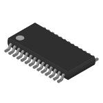
AD9215BRUZ-65
ActiveANALOG TO DIGITAL CONVERTER, 10 BIT, 65 MSPS, DIFFERENTIAL, SINGLE ENDED, PARALLEL, SINGLE, 2.7 V
Deep-Dive with AI
Search across all available documentation for this part.

AD9215BRUZ-65
ActiveANALOG TO DIGITAL CONVERTER, 10 BIT, 65 MSPS, DIFFERENTIAL, SINGLE ENDED, PARALLEL, SINGLE, 2.7 V
Deep-Dive with AI
Technical Specifications
Parameters and characteristics for this part
| Specification | AD9215BRUZ-65 |
|---|---|
| Architecture | Pipelined |
| Configuration | S/H-ADC |
| Data Interface | Parallel |
| Input Type | Single Ended, Differential |
| Mounting Type | Surface Mount |
| Number of A/D Converters | 1 |
| Number of Bits [custom] | 10 |
| Number of Inputs | 1 |
| Operating Temperature [Max] | 85 °C |
| Operating Temperature [Min] | -40 °C |
| Package / Case | 28-TSSOP |
| Package / Case | 0.173 in |
| Package / Case [y] | 4.4 mm |
| Ratio - S/H:ADC | 1:1 |
| Reference Type | Internal |
| Sampling Rate (Per Second) | 65 M |
| Supplier Device Package | 28-TSSOP |
| Voltage - Supply, Analog [Max] | 3.3 V |
| Voltage - Supply, Analog [Min] | 2.7 V |
| Voltage - Supply, Digital [Max] | 3.6 V |
| Voltage - Supply, Digital [Min] | 2.25 V |
Pricing
Prices provided here are for design reference only. For realtime values and availability, please visit the distributors directly
Description
General part information
AD9215 Series
The AD9215 is a family of monolithic, single 3 V supply, 10-bit, 65/80/105 MSPS analog-to-digital converters (ADC). This family features a high performance sample-and-hold amplifier (SHA) and voltage reference. The AD9215 uses a multistage differential pipelined architecture with output error correction logic to provide 10-bit accuracy at 105 MSPS data rates and to guarantee no missing codes over the full operating temperature range.The wide bandwidth, truly differential sample-and-hold amplifier (SHA) allows for a variety of user-selectable input ranges and offsets including single-ended applications. It is suitable for multiplexed systems that switch full-scale voltage levels in successive channels and for sampling single-channel inputs at frequencies well beyond the Nyquist rate. Combined with power and cost savings over previously available ADCs, the AD9215 is suitable for applications in communications, imaging, and medical ultrasound.A single-ended clock input is used to control all internal conversion cycles. A duty cycle stabilizer compensates for wide variations in the clock duty cycle while maintaining excellent performance. The digital output data is presented in straight binary or twos complement formats. An out-of-range signal indicates an overflow condition, which can be used with the MSB to determine low or high overflow.Fabricated on an advanced CMOS process, the AD9215 is available in both a 28-lead surface-mount plastic package and a 32-lead chip scale package and is specified over the industrial temperature range of −40°C to +85°C.PRODUCT HIGHLIGHTSThe AD9215 operates from a single 3 V power supply and features a separate digital output driver supply to accommodate 2.5 V and 3.3 V logic families.Operating at 105 MSPS, the AD9215 core ADC consumes a low 120 mW; at 80 MSPS, the power dissipation is 104 mW; and at 65 MSPS, the power dissipation is 96 mW.The patented SHA input maintains excellent performance for input frequencies up to 200 MHz and can be configured for single-ended or differential operation.The AD9215 is part of several pin compatible 10-, 12-, and 14-bit low power ADCs. This allows a simplified upgrade from 10 bits to 12 bits for systems up to 80 MSPS.The clock duty cycle stabilizer maintains converter performance over a wide range of clock pulse widths.The out of range (OR) output bit indicates when the signal is beyond the selected input range.APPLICATIONSUltrasound equipmentIF sampling in communications receiversBattery-powered instrumentsHand-held scopemetersLow cost digital oscilloscopes
Documents
Technical documentation and resources


