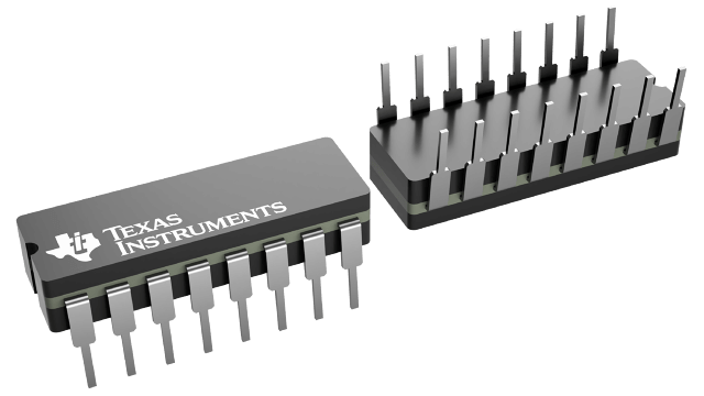
CD4076BF
ActiveFLIP FLOP D-TYPE BUS INTERFACE POS-EDGE 3-ST 1-ELEMENT 16-PIN CDIP TUBE
Deep-Dive with AI
Search across all available documentation for this part.

CD4076BF
ActiveFLIP FLOP D-TYPE BUS INTERFACE POS-EDGE 3-ST 1-ELEMENT 16-PIN CDIP TUBE
Deep-Dive with AI
Technical Specifications
Parameters and characteristics for this part
| Specification | CD4076BF |
|---|---|
| null | |
Pricing
Prices provided here are for design reference only. For realtime values and availability, please visit the distributors directly
| Distributor | Package | Quantity | $ | |
|---|---|---|---|---|
| Digikey | Bulk | 24 | $ 12.80 | |
| Texas Instruments | TUBE | 1 | $ 16.91 | |
| 100 | $ 14.77 | |||
| 250 | $ 11.39 | |||
| 1000 | $ 10.19 | |||
Description
General part information
CD4076B-MIL Series
CD4076B types are four-bit registers consisting of D-type flip-flops that feature three-state outputs. Data Disable inputs are provided to control the entry of data into the flip-flops. When both Data Disable inputs are low, data at the D inputs are loaded into their respective flip-flops on the next positive transition of the clock input. Output Disable inputs are also provided. When the Output Disable inputs are both low, the normal logic states of the four outputs are available to the load. The outputs are disabled independently of the clock by a high logic level at either Output Disable input, and present a high impedance.
The CD4076B types are supplied in 16-lead hermetic dual-in-line ceramic packages (F3A suffix), 16-lead dual-in-line plastic packages (E suffix), 16-lead small-outline packages (M, M96, MT and NSR suffixes), and 16-lead thin shrink small-outline packages (PW and PWR suffixes).
CD4076B types are four-bit registers consisting of D-type flip-flops that feature three-state outputs. Data Disable inputs are provided to control the entry of data into the flip-flops. When both Data Disable inputs are low, data at the D inputs are loaded into their respective flip-flops on the next positive transition of the clock input. Output Disable inputs are also provided. When the Output Disable inputs are both low, the normal logic states of the four outputs are available to the load. The outputs are disabled independently of the clock by a high logic level at either Output Disable input, and present a high impedance.
Documents
Technical documentation and resources


