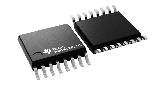
CDCVF25084PW
Active3.3-V X4 CLOCK MULTIPLIER WITH 8 OUTPUTS
Deep-Dive with AI
Search across all available documentation for this part.

CDCVF25084PW
Active3.3-V X4 CLOCK MULTIPLIER WITH 8 OUTPUTS
Deep-Dive with AI
Technical Specifications
Parameters and characteristics for this part
| Specification | CDCVF25084PW |
|---|---|
| Differential - Input:Output | False |
| Divider/Multiplier | No |
| Divider/Multiplier | Yes |
| Frequency - Max [Max] | 180 MHz |
| Mounting Type | Surface Mount |
| Number of Circuits | 1 |
| Operating Temperature [Max] | 85 °C |
| Operating Temperature [Min] | -40 °C |
| Output | LVTTL |
| Package / Case | 16-TSSOP |
| Package / Case [x] | 0.173 in |
| Package / Case [y] | 4.4 mm |
| PLL | Yes with Bypass |
| Ratio - Input:Output [custom] | 8 |
| Ratio - Input:Output [custom] | 2 |
| Supplier Device Package | 16-TSSOP |
| Type | PLL Clock Multiplier |
| Voltage - Supply [Max] | 3.6 V |
| Voltage - Supply [Min] | 3 V |
Pricing
Prices provided here are for design reference only. For realtime values and availability, please visit the distributors directly
| Distributor | Package | Quantity | $ | |
|---|---|---|---|---|
| Digikey | Tube | 180 | $ 8.42 | |
| Texas Instruments | TUBE | 1 | $ 8.62 | |
| 100 | $ 7.03 | |||
| 250 | $ 5.52 | |||
| 1000 | $ 4.68 | |||
Description
General part information
CDCVF25084 Series
The CDCVF25084 is a high-performance, low-skew, low-jitter, phase-lock loop clock multiplier. It uses a PLL to precisely align, in both frequency and phase, the output clocks to the input clock signal including a multiplication factor of four. The CDCVF25084 operates from a nominal supply voltage of 3.3 V. The device also includes integrated series-damping resistors in the output drivers that make it ideal for driving point-to-point loads.
Two banks of four outputs each provide low-skew, low-jitter copies of CLKIN x four. All outputs operate at the same frequency. Output duty cycles are adjusted to 50%, independent of duty cycle at CLKIN. The device automatically goes into power-down mode when no input signal is applied to CLKIN and the outputs go into a low state. Unlike many products containing PLLs, the CDCVF25084 does not require an external RC network. The loop filter for the PLL is included on-chip, minimizing component count, space, and cost.
Because it is based on a PLL circuitry, the CDCVF25084 requires a stabilization time to achieve phase lock of the feedback signal to the reference signal. This stabilization is required following power up and application of a fixed-frequency signal at CLKIN and any following changes to the PLL reference.
Documents
Technical documentation and resources


