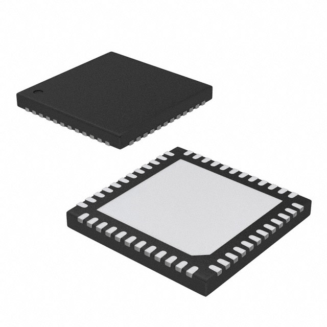
ADCLK854BCPZ
Active1.8 V, 12-LVDS/24-CMOS OUTPUT, LOW POWER CLOCK FANOUT BUFFER
Deep-Dive with AI
Search across all available documentation for this part.

ADCLK854BCPZ
Active1.8 V, 12-LVDS/24-CMOS OUTPUT, LOW POWER CLOCK FANOUT BUFFER
Deep-Dive with AI
Technical Specifications
Parameters and characteristics for this part
| Specification | ADCLK854BCPZ |
|---|---|
| Differential - Input:Output [custom] | True |
| Differential - Input:Output [custom] | True |
| Frequency - Max [Max] | 1.2 GHz |
| Input | CML, CMOS, LVPECL, HSTL, LVDS |
| Mounting Type | Surface Mount |
| Number of Circuits | 1 |
| Operating Temperature [Max] | 85 °C |
| Operating Temperature [Min] | -40 °C |
| Output | CMOS, LVDS |
| Package / Case | 48-VFQFN Exposed Pad, CSP |
| Ratio - Input:Output | 2:12 |
| Supplier Device Package | 48-LFCSP-VQ |
| Supplier Device Package [x] | 7 |
| Supplier Device Package [y] | 6.75 |
| Type | Fanout Buffer (Distribution), Multiplexer |
| Voltage - Supply [Max] | 1.89 V |
| Voltage - Supply [Min] | 1.71 V |
Pricing
Prices provided here are for design reference only. For realtime values and availability, please visit the distributors directly
| Distributor | Package | Quantity | $ | |
|---|---|---|---|---|
| Digikey | Tray | 1 | $ 15.51 | |
| 10 | $ 10.83 | |||
| 76 | $ 8.46 | |||
| 152 | $ 8.21 | |||
Description
General part information
ADCLK854 Series
The ADCLK854 is a 1.2 GHz/250 MHz LVDS/CMOS fanout buffer optimized for low jitter and low power operation. Possible configurations range from 12 LVDS to 24 CMOS outputs, including combinations of LVDS and CMOS outputs. Three control lines are used to determine whether fixed blocks of outputs (three banks of four) are LVDS or CMOS outputs.The ADCLK854 offers two selectable inputs and a sleep mode feature. The IN_SEL pin state determines which input is fanned out to all the outputs. The SLEEP pin enables a sleep mode to power down the device.The inputs accept various types of single-ended and differential logic levels including LVPECL, LVDS, HSTL, CML, and CMOS. Table 8 provides interface options for each type of connection.This device is available in a 48-pin LFCSP package. It is specified for operation over the standard industrial temperature range of −40°C to +85°C.APPLICATIONSLow jitter clock distributionClock and data signal restorationLevel translationWireless communicationsWired communicationsMedical and industrial imagingATE and high performance instrumentation
Documents
Technical documentation and resources


