Deep-Dive with AI
Search across all available documentation for this part.

Deep-Dive with AI
Technical Specifications
Parameters and characteristics for this part
| Specification | AD75019JP |
|---|---|
| -3db Bandwidth | 20 MHz |
| Applications | Analog |
| Features | Serial Interface |
| Mounting Type | Surface Mount |
| Multiplexer/Demultiplexer Circuit [custom] | 16 |
| Multiplexer/Demultiplexer Circuit [custom] | 16 |
| Number of Channels | 1 |
| On-State Resistance (Max) [Max] | 300 Ohm |
| Operating Temperature [Max] | 85 C |
| Operating Temperature [Min] | -25 °C |
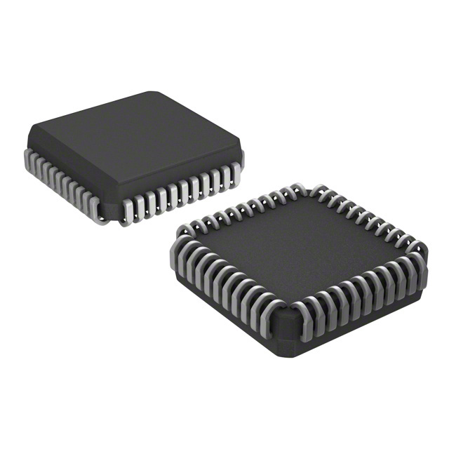
| Package / Case | 44-LCC (J-Lead) |
| Supplier Device Package | 44-PLCC (16.59x16.59) |
| Voltage - Supply, Dual (V±) [Max] | 12 V |
| Voltage - Supply, Dual (V±) [Min] | -12 V |
| Voltage - Supply, Single (V+) [Max] | 25.2 V |
| Voltage - Supply, Single (V+) [Min] | 9 V |
Pricing
Prices provided here are for design reference only. For realtime values and availability, please visit the distributors directly
| Distributor | Package | Quantity | $ | |
|---|---|---|---|---|
Description
General part information
AD75019 Series
The AD75019 contains 256 analog switches in a 16 × 16 array. Any of the X or Y pins may serve as an input or output. Any or all of the X terminals may be programmed to connect to any or all of the Y terminals. The switches can accommodate signals with amplitudes up to the supply rails and have a typical on-resistance of 150 Ω.Data is loaded serially via the SIN input and clocked into an on-board 256-bit shift register via SCLK. When all the switch settings have been programmed, data is transferred into a set of 256 latches via PCLK. The serial shift register is dynamic, so there is a minimum clock rate of 20 kHz. The maximum clock rate of 5 MHz allows loading times as short as 52 μs. The switch control latches are static and will hold their data as long as power is applied.To extend the number of switches in the array, you may cascade multiple AD75019s. The SOUT output is the end of the shift register, and may be connected to the SIN input of the next AD75019.The AD75019 is fabricated in Analog Devices’ BiMOS II process. This epitaxial BiCMOS process features CMOS devices for low distortion switches and bipolar devices for ESD protection.
Documents
Technical documentation and resources


