Deep-Dive with AI
Search across all available documentation for this part.

Deep-Dive with AI
Technical Specifications
Parameters and characteristics for this part
| Specification | AD637JR-REEL7 |
|---|---|
| Current - Supply | 2.2 mA |
| Mounting Type | Surface Mount |
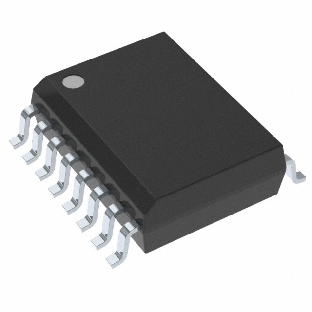
| Package / Case | 16-SOIC |
| Package / Case [x] | 0.295 in |
| Package / Case [y] | 7.5 mm |
| Supplier Device Package | 16-SOIC |
| Voltage - Supply [Max] | 18 V |
| Voltage - Supply [Min] | -3 V |
Pricing
Prices provided here are for design reference only. For realtime values and availability, please visit the distributors directly
| Distributor | Package | Quantity | $ | |
|---|---|---|---|---|
Description
General part information
AD637 Series
The AD637 is a complete, high accuracy, rms-to-dc converter that computes the true rms value of any complex waveform. It offers performance that is unprecedented in integrated circuit rms-to-dc converters and comparable to discrete and modular techniques in accuracy, bandwidth, and dynamic range. The AD637 computes the true root mean square, mean square, or absolute value of any complex ac (or ac plus dc) input waveform and gives an equivalent dc output voltage. The true rms value of a waveform is more useful than an average rectified signal because it relates directly to the power of the signal. The rms value of a statistical signal relates to the standard deviation of the signal.Superior crest factor compensation permits measurements of signals with crest factors of up to 10 with less than 1% additional error. The wide bandwidth of the AD637 permits the measurement of signals up to 600 kHz with inputs of 200 mV rms and up to 8 MHz when the input levels are above 1 V rms.Direct dB value of the rms output with a range of 60 dB is available on a separate pin. An externally programmed reference current allows the user to select the 0 dB reference voltage to correspond to any level between 0.1 V and 2.0 V rms.A chip select connection on the AD637 permits the user to decrease the supply current from 2.2 mA to 350 µA during periods when the rms function is not in use. This feature facilitates the addition of precision rms measurement to remote or handheld applications where minimum power consumption is critical. In addition, when the AD637 is powered down, the output goes to a high impedance state. This allows several AD637s to be tied together to form a wideband true rms multiplexer.The input circuitry of the AD637 is protected from overload voltages in excess of the supply levels. The inputs are not damaged by input signals if the supply voltages are lost.The AD637 is laser wafer trimmed to achieve rated performance without external trimming. The only external component required is a capacitor that sets the averaging period. The value of this capacitor also determines low frequency accuracy, ripple level, and settling time.The on-chip buffer amplifier is used either as an input buffer or in an active filter configuration. The filter can be used to reduce the amount of ac ripple, thereby increasing accuracy.The AD637 is available in accuracy Grade J and Grade K for commercial temperature range (0°C to 70°C) applications, accuracy Grade A and Grade B for industrial range (−40°C to +85°C) applications, and accuracy Grade S rated over the −55°C to +125°C temperature range. All versions are available in hermetically sealed, 14-lead SBDIP, 14-lead CERDIP, and 16-lead SOIC_W packages.
Documents
Technical documentation and resources


