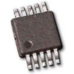
ADG1422BRMZ
Active2.1 Ω MAXIMUM ON RESISTANCE, ±15 V/+12/±5 VICMOS DUAL SPST SWITCHES
Deep-Dive with AI
Search across all available documentation for this part.

ADG1422BRMZ
Active2.1 Ω MAXIMUM ON RESISTANCE, ±15 V/+12/±5 VICMOS DUAL SPST SWITCHES
Technical Specifications
Parameters and characteristics for this part
| Specification | ADG1422BRMZ |
|---|---|
| -3db Bandwidth | 180 MHz |
| Channel Capacitance (CS(off), CD(off)) [custom] | 18 pF |
| Channel Capacitance (CS(off), CD(off)) [custom] | 22 pF |
| Channel-to-Channel Matching (ΔRon) | 20 mOhm |
| Charge Injection | -5 pC |
| Crosstalk | -74 dB |
| Current - Leakage (IS(off)) (Max) | 500 pA |
| Mounting Type | Surface Mount |
| Multiplexer/Demultiplexer Circuit | 1:1 |
| Number of Circuits | 2 |
| On-State Resistance (Max) [Max] | 2.4 Ohm |
| Operating Temperature [Max] | 125 °C |
| Operating Temperature [Min] | -40 °C |
| Package / Case | 10-MSOP, 10-TFSOP |
| Package / Case [x] | 3 mm |
| Package / Case [x] | 0.118 in |
| Supplier Device Package | 10-MSOP |
| Switch Circuit | SPST - NC |
| Switch Time (Ton, Toff) (Max) [custom] | 145 ns |
| Switch Time (Ton, Toff) (Max) [custom] | 145 ns |
| Voltage - Supply, Dual (V±) [Max] | 16.5 V |
| Voltage - Supply, Dual (V±) [Min] | -4.5 V |
| Voltage - Supply, Single (V+) [Max] | 16.5 V |
| Voltage - Supply, Single (V+) [Min] | 5 V |
Pricing
Prices provided here are for design reference only. For realtime values and availability, please visit the distributors directly
Description
General part information
ADG1422 Series
TheADG1421/ ADG1422 /ADG1423contain two independent single-pole/single-throw (SPST) switches. The ADG1421 and ADG1422 differ only in that the digital control logic is inverted. The ADG1421 switches are turned on with Logic 1 on the appropriate control input, and Logic 0 is required for the ADG1422. The ADG1423 has one switch with digital control logic similar to that of the ADG1421; the logic is inverted on the other switch. The ADG1423 exhibits break-before-make switching action for use in multiplexer applications. Each switch conducts equally well in both directions when on and has an input signal range that extends to the supplies. In the off condition, signal levels up to the supplies are blocked.TheiCMOS®(industrial CMOS) modular manufacturing process combines high voltage, complementary metal-oxide semiconductor (CMOS) and bipolar technologies. It enables the development of a wide range of high performance analog ICs capable of 33 V operation in a footprint that no other generation of high voltage parts has achieved. Unlike analog ICs using conventional CMOS processes,iCMOS components can tolerate high supply voltages while providing increased performance, dramatically lower power consumption, and reduced package size.The on resistance profile is very flat over the full analog input range ensuring excellent linearity and low distortion when switching audio signals. TheiCMOS construction ensures ultralow power dissipation, making the part ideally suited for portable and battery-powered instruments.PRODUCT HIGHLIGHTS2.4 Ω maximum on resistance at 25°C.Minimum distortion.3 V logic-compatible digital inputs: VINH= 2.0 V, VINL= 0.8 V.No VLlogic power supply required.10-lead MSOP and 10-lead, 3 mm × 3 mm LFCSP packages.APPLICATIONSAutomatic test equipmentData acquisition systemsRelay replacementsBattery-powered systemsSample-and-hold systemsAudio signal routingVideo signal routingCommunication systems
Documents
Technical documentation and resources


