HMC842LC4B
Obsolete45 GBPS FANOUT BUFFER WITH PROGRAMMABLE OUTPUT VOLTAGE
Deep-Dive with AI
Search across all available documentation for this part.

HMC842LC4B
Obsolete45 GBPS FANOUT BUFFER WITH PROGRAMMABLE OUTPUT VOLTAGE
Deep-Dive with AI
Technical Specifications
Parameters and characteristics for this part
| Specification | HMC842LC4B |
|---|---|
| Mounting Type | Surface Mount |
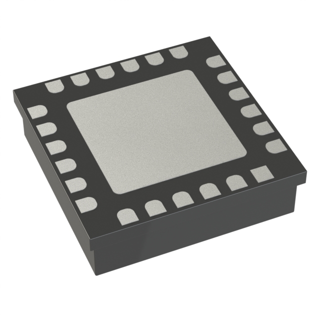
| Package / Case | 24-TFQFN Exposed Pad |
| Supplier Device Package | 24-QFN (4x4) |
Pricing
Prices provided here are for design reference only. For realtime values and availability, please visit the distributors directly
| Distributor | Package | Quantity | $ | |
|---|---|---|---|---|
Description
General part information
HMC842 Series
The HMC842LC4B is a 1:2 Fanout Buffer designed to support data transmission rates up to 45 Gbps. The device can also operate with clock signals up to 28 GHz. During normal operation, input data (or clock) is transferred to both output channels. Differential input and output signals of the HMC842LC4B are terminated with 50 Ohms to ground on-chip, and may be either AC or DC coupled. The Outputs can be connected directly to a 50 Ohms-to-ground terminated system, while DC blocking capacitors should be used if the terminating system is 50 Ohms to a non-ground DC voltage.The HMC842LC4B also features two separate output level control pins, VAC1 and VAC2 which provide loss compensation and signal level optimization for each output channel independently. The HMC842LC4B operates from a single -3.3V DC supply and is available in a ceramic RoHS compliant 4x4 mm SMT package.ApplicationsOC-768 & SDH STM-256 EquipmentRF ATE ApplicationsShort, intermediate, & Long Haul Fiber Optic ApplicationsBroadband Test & MeasurementSerial Data Transmission up to 45 GbpsClock Buffering up to 28 GHz
Documents
Technical documentation and resources


