Deep-Dive with AI
Search across all available documentation for this part.

Deep-Dive with AI
Technical Specifications
Parameters and characteristics for this part
| Specification | NB3N51044DTG |
|---|---|
| Differential - Input:Output | No/Yes |
| Divider/Multiplier | Yes/No |
| Frequency - Max [Max] | 125 MHz |
| Input | Crystal, Clock |
| Mounting Type | Surface Mount |
| Number of Circuits | 1 |
| Operating Temperature [Max] | 85 °C |
| Operating Temperature [Min] | -40 °C |
| Output | LVDS, HCSL |
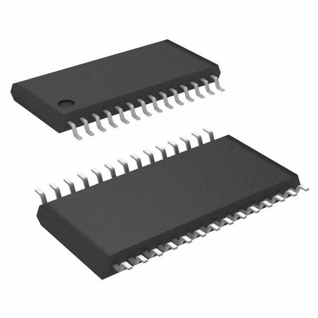
| Package / Case | 28-TSSOP |
| Package / Case | 0.173 in |
| Package / Case [y] | 4.4 mm |
| PLL | Yes with Bypass |
| Ratio - Input:Output [custom] | 2:4 |
| Supplier Device Package | 28-TSSOP |
| Voltage - Supply [Max] | 3.465 V |
| Voltage - Supply [Min] | 3.135 V |
Pricing
Prices provided here are for design reference only. For realtime values and availability, please visit the distributors directly
| Distributor | Package | Quantity | $ | |
|---|---|---|---|---|
Description
General part information
NB3N51044 Series
The NB3N51044 is a precision, low phase noise clock generator that supports PCI Express and sRIO clock requirements. The device accepts a 25 MHz fundamental mode parallel resonant crystal or a 25 MHz single ended reference clock signal and generates four differential HCSL/LVDS outputs of 100 MHz or 125 MHz clock frequency based on frequency select input F_SEL. NB3N51044 is configurable to bypass the PLL from signal path using BYPASS, and provides the output frequency through the divider network. All clock outputs can be individually enabled / disabled through hardware input pins OE. In addition, device can be reset using Master Reset input pin MR_OE#.
Documents
Technical documentation and resources


