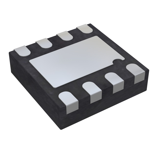
AD5683RACPZ-RL7
ActiveTINY 16-BIT SPINANODAC+, WITH ±2 (16-BIT) LSB INL AND 2PPM/°C REFERENCE
Deep-Dive with AI
Search across all available documentation for this part.

AD5683RACPZ-RL7
ActiveTINY 16-BIT SPINANODAC+, WITH ±2 (16-BIT) LSB INL AND 2PPM/°C REFERENCE
Deep-Dive with AI
Technical Specifications
Parameters and characteristics for this part
| Specification | AD5683RACPZ-RL7 |
|---|---|
| Architecture | String DAC |
| Data Interface | SPI |
| Differential Output | False |
| INL/DNL (LSB) | ±8, ±1 |
| Mounting Type | Surface Mount |
| Number of Bits | 16 |
| Operating Temperature [Max] | 105 ░C |
| Operating Temperature [Min] | -40 °C |
| Output Type | Voltage - Buffered |
| Package / Case | 8-UFDFN Exposed Pad, CSP |
| Reference Type | External, Internal |
| Settling Time | 7 µs |
| Supplier Device Package | 8-LFCSP-UD (2x2) |
| Voltage - Supply, Analog [Max] | 5.5 V |
| Voltage - Supply, Analog [Min] | 2.7 V |
| Voltage - Supply, Digital [Max] | 5.5 V |
| Voltage - Supply, Digital [Min] | 2.7 V |
Pricing
Prices provided here are for design reference only. For realtime values and availability, please visit the distributors directly
| Distributor | Package | Quantity | $ | |
|---|---|---|---|---|
| Digikey | Cut Tape (CT) | 1 | $ 9.44 | |
| 10 | $ 6.38 | |||
| 25 | $ 5.59 | |||
| 100 | $ 4.69 | |||
| 250 | $ 4.25 | |||
| 500 | $ 4.24 | |||
| 1000 | $ 4.32 | |||
| Digi-Reel® | 1 | $ 9.44 | ||
| 10 | $ 6.38 | |||
| 25 | $ 5.59 | |||
| 100 | $ 4.69 | |||
| 250 | $ 4.25 | |||
| 500 | $ 4.24 | |||
| 1000 | $ 4.32 | |||
| Tape & Reel (TR) | 3000 | $ 4.24 | ||
Description
General part information
AD5683R Series
The AD5683R/AD5682R/AD5681R/AD5683, members of thenanoDAC+®family, are low power, single-channel, 16-/14-/12-bit buffered voltage out digital-to-analog converters (DACs). The devices, except the AD5683, include an enabled by default internal 2.5 V reference, offering 2 ppm/°C drift. The output span can be programmed to be 0 V to VREFor 0 V to 2 × VREF. All devices operate from a single 2.7 V to 5.5 V supply and are guaranteed monotonic by design. The devices are available in a 2.00 mm × 2.00 mm, 8-lead LFCSP or a 10-lead MSOP.The internal power-on reset circuit ensures that the DAC register is written to zero scale at power-up while the internal output buffer is configured in normal mode. The AD5683R/AD5682R/AD5681R/AD5683 contain a power-down mode that reduces the current consumption of the device to 2 µA (maximum) at 5 V and provides software selectable output loads while in power-down mode.The AD5683R/AD5682R/AD5681R/AD5683 use a versatile 3-wire serial interface that operates at clock rates of up to 50 MHz. Some devices also include asynchronousRESETpin and VLOGICpin options, allowing 1.8 V compatibilityProduct HighlightsHigh Relative Accuracy (INL).AD5683R/AD5683 (16-bit): ±2 LSB maximum.Low Drift, 2.5 V On-Chip Reference.2 ppm/°C typical temperature coefficient.5 ppm/°C maximum temperature coefficient.Two Package Options.2.00 mm × 2.00 mm, 8-lead LFCSP.10-lead MSOP.ApplicationsProcess controlsData acquisition systemsDigital gain and offset adjustmentProgrammable voltage sources
Documents
Technical documentation and resources


