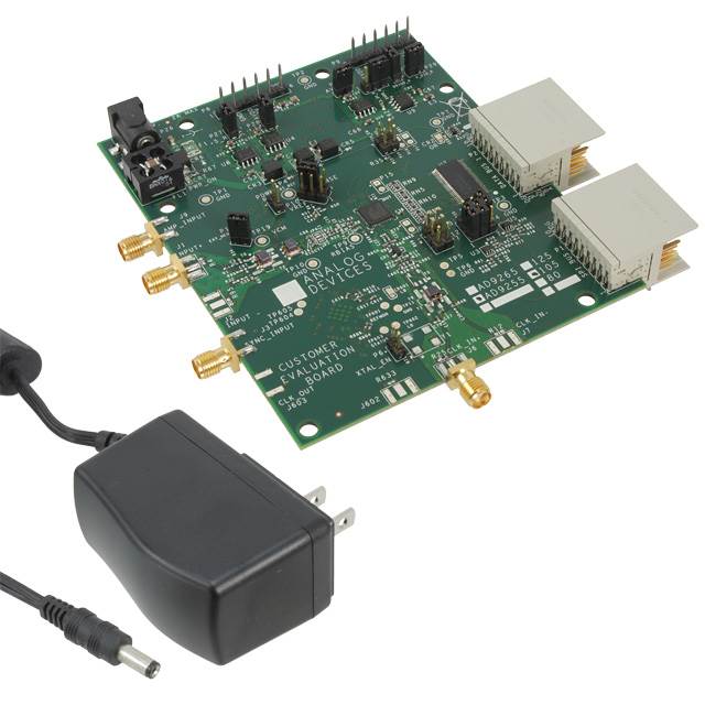
AD9255-105EBZ
ObsoleteBOARD EVALUATION 105MSPS AD9255

AD9255-105EBZ
ObsoleteBOARD EVALUATION 105MSPS AD9255
Technical Specifications
Parameters and characteristics for this part
| Specification | AD9255-105EBZ |
|---|---|
| Data Interface | SPI |
| Input Range [Max] | 2 Vpp |
| Input Range [Min] | 1 Vpp |
| Number of A/D Converters | 1 |
| Number of Bits | 14 |
| Power (Typ) @ Conditions | 371 mW |
| Sampling Rate (Per Second) | 105 M |
| Supplied Contents | Board(s) |
| Utilized IC / Part | AD9255 |
Pricing
Prices provided here are for design reference only. For realtime values and availability, please visit the distributors directly
| Distributor | Package | Quantity | $ | |
|---|---|---|---|---|
Description
General part information
AD9255 Series
The AD9255 is a 14-bit, 125 MSPS analog-to-digital converter (ADC). The AD9255 is designed to support communications applications where high performance combined with low cost, small size, and versatility is desired.The ADC core features a multistage, differential pipelined architecture with integrated output error correction logic to provide 14-bit accuracy at 125 MSPS data rates and guarantees no missing codes over the full operating temperature range.The ADC features a wide bandwidth differential sample-and-hold analog input amplifier supporting a variety of user-selectable input ranges. It is suitable for multiplexed systems that switch full-scale voltage levels in successive channels and for sampling single-channel inputs at frequencies well beyond the Nyquist rate. Combined with power and cost savings over previously available ADCs, the AD9255 is suitable for applications in communications, instrumentation, and medical imaging.A differential clock input controls all internal conversion cycles. A duty cycle stabilizer provides the means to compensate for variations in the ADC clock duty cycle, allowing the converters to maintain excellent performance over a wide range of input clock duty cycles. An integrated voltage reference eases design considerations.The ADC output data format is either parallel 1.8 V CMOS or LVDS (DDR). A data output clock is provided to ensure proper latch timing with receiving logic.Programming for setup and control is accomplished using a 3-wire SPI-compatible serial interface. Flexible power-down options allow significant power savings, when desired. An optional on-chip dither function is available to improve SFDR performance with low power analog input signals.The AD9255 is available in a Pb-free, 48-lead LFCSP and is specified over the industrial temperature range of −40°C to +85°C.PRODUCT HIGHLIGHTSOn-chip dither option for improved SFDR performance with low power analog input.Proprietary differential input that maintains excellent SNR performance for input frequencies up to 300 MHz.Operation from a single 1.8 V supply and a separate digital output driver supply accommodating 1.8 V CMOS or LVDS outputs.Standard serial port interface (SPI) that supports various product features and functions, such as data formatting (offset binary, twos complement, or gray coding), enabling the clock DCS, power-down, test modes, and voltage reference mode.Pin compatibility with the AD9265, allowing a simple migration up to 16 bits.ApplicationsCommunicationsMultimode digital receivers (3G)GSM, EDGE, W-CDMA, LTE, CDMA2000, WiMAX, and TD-SCDMASmart antenna systemsGeneral-purpose software radiosBroadband data applicationsUltrasound equipment
Documents
Technical documentation and resources


