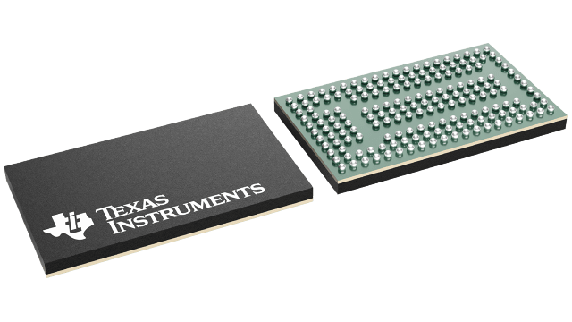
SN74SSQEA32882ZALR
Active810-MHZ, JEDEC SSTE32882 COMPLIANT 28-BIT TO 56-BIT REGISTERED BUFFER WITH ADDRESS-PARITY TEST
Deep-Dive with AI
Search across all available documentation for this part.

SN74SSQEA32882ZALR
Active810-MHZ, JEDEC SSTE32882 COMPLIANT 28-BIT TO 56-BIT REGISTERED BUFFER WITH ADDRESS-PARITY TEST
Technical Specifications
Parameters and characteristics for this part
| Specification | SN74SSQEA32882ZALR |
|---|---|
| Logic Type | 1:2 Registered Buffer with Parity |
| Mounting Type | Surface Mount |
| Number of Bits | 56, 28 |
| Operating Temperature [Max] | 85 °C |
| Operating Temperature [Min] | 0 °C |
| Package / Case | 176-TFBGA |
| Supplier Device Package | 13.5x8, 176-NFBGA |
Pricing
Prices provided here are for design reference only. For realtime values and availability, please visit the distributors directly
| Distributor | Package | Quantity | $ | |
|---|---|---|---|---|
| Digikey | Cut Tape (CT) | 1 | $ 8.25 | |
| Digi-Reel® | 1 | $ 8.25 | ||
| Tape & Reel (TR) | 2000 | $ 4.51 | ||
| Texas Instruments | LARGE T&R | 1 | $ 6.32 | |
| 100 | $ 5.15 | |||
| 250 | $ 4.05 | |||
| 1000 | $ 3.43 | |||
Description
General part information
SN74SSQEA32882 Series
This JEDEC SSTE32882-compliant, 28-bit 1:2 or 26-bit 1:2 and 4-bit 1:1 registering clock driver with parity is designed for operation on DDR3 registered DIMMs with VDDof 1.5 V and on DDR3L registered DIMMs with VDDof 1.35 V.
All inputs are 1.5 V and 1.35 V CMOS compatible. All outputs are CMOS drivers optimized to drive DRAM signals on terminated traces in DDR3 RDIMM applications. The clock outputs Yn andYnand control net outputs DxCKEn,DxCSnand DxODTn can be driven with a different strength and skew to optimize signal integrity, compensate for different loading and equalize signal travel speed.
The SN74SSQEA32882 has two basic modes of operation associated with the Quad Chip Select Enable (QCSEN) input. When theQCSENinput pin is open (or pulled high), the component has two chip select inputs,DCS0andDCS1, and two copies of each chip select output,QACS0,QACS1,QBCS0andQBCS1. This is the "QuadCS disabled" mode. When theQCSENinput pin is pulled low, the component has four chip select inputsDCS[3:0], and four chip select outputs,QCS[3:0]. This is the "QuadCS enabled" mode. Through the remainder of this specification,DCS[n:0]will indicate all of the chip select inputs, where n=1 for QuadCS disabled, and n=3 for QuadCS enabled.QxCS[n:0]will indicate all of the chip select outputs.
Documents
Technical documentation and resources


