Deep-Dive with AI
Search across all available documentation for this part.

Deep-Dive with AI
Technical Specifications
Parameters and characteristics for this part
| Specification | CD4013BPWRG4 |
|---|---|
| Clock Frequency | 24 MHz |
| Current - Output High, Low [custom] | 6.8 mA |
| Current - Output High, Low [custom] | 6.8 mA |
| Current - Quiescent (Iq) | 4 çA |
| Function | Reset, Set(Preset) |
| Input Capacitance | 5 pF |
| Max Propagation Delay @ V, Max CL | 90 ns |
| Mounting Type | Surface Mount |
| Number of Bits per Element | 1 |
| Number of Elements | 2 |
| Operating Temperature [Max] | 125 °C |
| Operating Temperature [Min] | -55 °C |
| Output Type | Complementary |
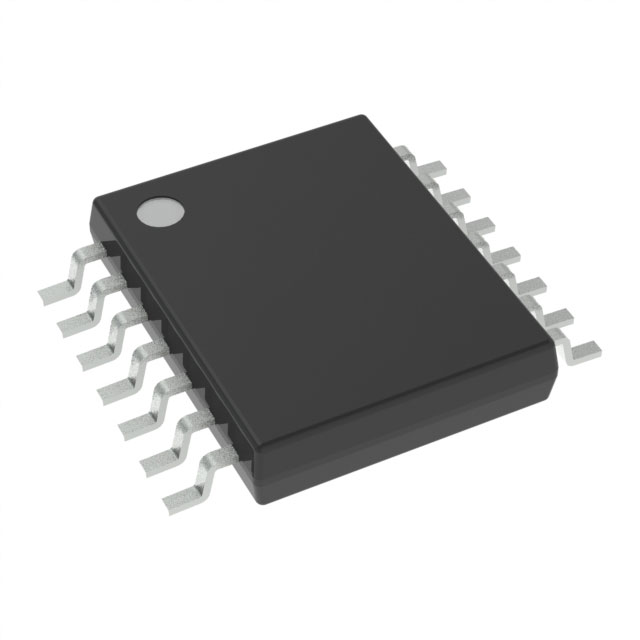
| Package / Case | 14-TSSOP |
| Package / Case [custom] | 0.173 " |
| Package / Case [custom] | 4.4 mm |
| Supplier Device Package | 14-TSSOP |
| Trigger Type | Positive Edge |
| Type | D-Type |
| Voltage - Supply [Max] | 18 V |
| Voltage - Supply [Min] | 3 V |
Pricing
Prices provided here are for design reference only. For realtime values and availability, please visit the distributors directly
| Distributor | Package | Quantity | $ | |
|---|---|---|---|---|
| Digikey | Tape & Reel (TR) | 2000 | $ 0.20 | |
| 6000 | $ 0.18 | |||
| 10000 | $ 0.17 | |||
| 50000 | $ 0.16 | |||
Description
General part information
CD4013B Series
The CD4013B device consists of two identical, independent data-type flip-flops. Each flip-flop has independent data, set, reset, and clock inputs and Q andQoutputs. These devices can be used for shift register applications, and, by connectingQoutput to the data input, for counter and toggle applications. The logic level present at the D input is transferred to the Q output during the positive-going transition of the clock pulse. Setting or resetting is independent of the clock and is accomplished by a high level on the set or reset line, respectively.
The CD4013B types are supplied in 14-pin dual-in-line plastic packages (E suffix), 14-pin small-outline packages (M, MT, M96, and NSR suffixes), and 14-pin thin shrink small-outline packages (PW and PWR suffixes).
The CD4013B device consists of two identical, independent data-type flip-flops. Each flip-flop has independent data, set, reset, and clock inputs and Q andQoutputs. These devices can be used for shift register applications, and, by connectingQoutput to the data input, for counter and toggle applications. The logic level present at the D input is transferred to the Q output during the positive-going transition of the clock pulse. Setting or resetting is independent of the clock and is accomplished by a high level on the set or reset line, respectively.
Documents
Technical documentation and resources
No documents available


