Deep-Dive with AI
Search across all available documentation for this part.

Deep-Dive with AI
Technical Specifications
Parameters and characteristics for this part
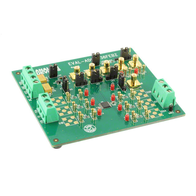
| Specification | EVAL-ADG5436FEBZ |
|---|---|
| Contents | Board(s) |
| Function | Analog Switch |
| Primary Attributes | 2 Inputs |
| Primary Attributes | SPDT Analog Switch |
| Supplied Contents | Board(s) |
| Type | Interface |
| Utilized IC / Part | ADG5436F |
Pricing
Prices provided here are for design reference only. For realtime values and availability, please visit the distributors directly
| Distributor | Package | Quantity | $ | |
|---|---|---|---|---|
| Digikey | Box | 1 | $ 77.35 | |
Description
General part information
ADG5436F Series
The ADG5436F is an analog multiplexer, containing two independently selectable single-pole, double-throw (SPDT) switches. An EN input is used to disable all the switches. For use in multiplexer applications, both switches exhibit break-before-make switching action.Each channel conducts equally well in both directions when on, and each switch has an input signal range that extends to the supplies. The digital inputs are compatible with 3 V logic inputs over the full operating supply range.When no power supplies are present, the switch remains in the off condition, and the channel inputs are high impedance. Under normal operating conditions, if the analog input signal level on any Sxx pin exceeds VDDor VSSby a threshold voltage, VT, the channel turns off and that Sxx pin becomes high impedance. If the channel is on, the drain pin reacts according to the drain response (DR) input pin. If the DR pin is left floating or pulled high, the drain remains high impedance and floats. If the DR pin is pulled low, the drain pulls to the exceeded rail. Input signal levels of up to +55 V or −55 V relative to ground are blocked, in both the powered and unpowered conditions. The low on resistance of the ADG5436F, combined with the on-resistance flatness over a significant portion of the signal range, makes it an ideal solution for data acquisition and gain switching applications where excellent linearity and low distortion are critical.Note that, throughout this data sheet, the dual function pin names are referenced only by the relevant function where applicable. See the Pin Configuration and Function Descriptions section for full pin names and function descriptions.Product HighlightsSource pins are protected against voltages greater than the supply rails, up to −55 V and +55 V.Source pins are protected against voltages between −55 V and +55 V in an unpowered state.Overvoltage detection with digital output indicates the operating state of the switches.Trench isolation guards against latch-up.Optimized for low on resistance and on-resistance flatness.The ADG5436F operates from a dual supply of ±5 V up to ±22 V, or a single power supply of 8 V up to 44 V.ApplicationsAnalog input/output modulesProcess control/distributed control systemsData acquisitionInstrumentationAvionicsAutomatic test equipmentCommunication systemsRelay replacement
Documents
Technical documentation and resources


