Deep-Dive with AI
Search across all available documentation for this part.

Deep-Dive with AI
Technical Specifications
Parameters and characteristics for this part
| Specification | AD1893JNZ |
|---|---|
| Applications | Digital Audio Interfacing |
| Function | Sample Rate Converter |
| Interface | Serial |
| Mounting Type | Through Hole |
| Number of Channels [custom] | 2 |
| Operating Temperature [Max] | 70 °C |
| Operating Temperature [Min] | -40 °C |
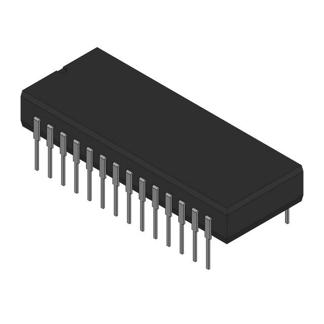
| Package / Case | 20-DIP |
| Package / Case | 7.62 mm |
| Package / Case | 0.3 in |
| Supplier Device Package | 20-DIP |
| Voltage - Supply [Max] | 5.5 V |
| Voltage - Supply [Min] | 2.7 V |
Pricing
Prices provided here are for design reference only. For realtime values and availability, please visit the distributors directly
| Distributor | Package | Quantity | $ | |
|---|---|---|---|---|
| Digikey | Bulk | 18 | $ 17.33 | |
Description
General part information
AD1893 Series
The AD1893 SamplePort is a fully digital, stereo Asynchronous Sample Rate Converter (ASRC) that solves sample rate interfacing and compatibility problems in digital audio equipment. The AD1893 is intended for 16-bit, low cost, non-varispeed applications where low voltage, low power operation is required. (Refer to theAD1890/AD1891data sheet for other products in the SamplePort family.) This device is asynchronous because the frequency and phase relationships between the input and output sample clocks (both are inputs to the AD1893 ASRC) are arbitrary and need not be related by a simple integer ratio. There is no need to explicitly select or program the input and output sample clock frequencies, as the AD1893 automatically senses the relationship between the two clocks. The input and output sample clock frequencies can nominally range from 8 kHz to 56 kHz, and the ratio between them can vary from approximately 1:2 to 2:1.The input and output control signals allow for considerable flexibility for interfacing to a variety of DSP chips, AES/EBU receivers and transmitters and for I2S compatible devices. Input and output data can be independently right- or left- (with or without a one bit clock delay) justified to the left/right clock edge. In the right-justified mode, the MSB is delayed 16 bit clock periods from the left/right clock edge transition. Input and output data can also be independently justified to the word clock rising edge. The data justification options are encoded on two mode pins for both the input port and the output port.The AD1893 is fabricated in a 0.8 µm single poly, double metal CMOS process and are packaged in a 0.6" wide 28-pin plastic DIP and a 10 mm by 10 mm body size 44-pin TQFP. The AD1893 operates from a +3 V to +5 V power supply over the temperature range of 0°C to +70°C.


