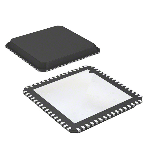
AD5391BCPZ-3
Active16-CHANNEL 3V/5V SERIAL INPUT SINGLE-SUPPLY 12-BIT VOLTAGE-OUTPUT
Deep-Dive with AI
Search across all available documentation for this part.

AD5391BCPZ-3
Active16-CHANNEL 3V/5V SERIAL INPUT SINGLE-SUPPLY 12-BIT VOLTAGE-OUTPUT
Deep-Dive with AI
Technical Specifications
Parameters and characteristics for this part
| Specification | AD5391BCPZ-3 |
|---|---|
| Architecture | String DAC |
| Data Interface | DSP, SPI, I2C |
| Differential Output | False |
| INL/DNL (LSB) | ±1 (Max) |
| Mounting Type | Surface Mount |
| Number of Bits | 12 bits |
| Number of D/A Converters | 16 D/A Converters |
| Operating Temperature [Max] | 85 °C |
| Operating Temperature [Min] | -40 °C |
| Output Type | Voltage - Buffered |
| Package / Case | 64-VFQFN Exposed Pad, CSP |
| Reference Type | External, Internal |
| Settling Time | 8 µs |
| Supplier Device Package | 64-LFCSP-VQ (9x9) |
| Voltage - Supply, Analog [Max] | 3.6 V |
| Voltage - Supply, Analog [Min] | 2.7 V |
| Voltage - Supply, Digital [Max] | 5.5 V |
| Voltage - Supply, Digital [Min] | 2.7 V |
Pricing
Prices provided here are for design reference only. For realtime values and availability, please visit the distributors directly
| Distributor | Package | Quantity | $ | |
|---|---|---|---|---|
| Digikey | Tray | 1 | $ 54.57 | |
| 10 | $ 42.32 | |||
| 25 | $ 39.19 | |||
| 80 | $ 36.18 | |||
| 230 | $ 36.16 | |||
Description
General part information
AD5391 Series
The AD5390 / AD5391 are complete single-supply, 16-channel, 14-bit and 12-bit DACs, respectively. The AD5392 is a complete single-supply, 8-channel, 14-bit DAC. The devices are available in either a 64-lead LFCSP or a 52-lead LQFP. All channels have an on-chip output amplifier with rail-to-rail operation. All devices include an internal 1.25/2.5 V, 10 ppm/°C reference, an on-chip channel monitor function that multiplexes the analog outputs to a common MON_OUT pin for external monitoring, and an output amplifier boost mode that optimizes the output amplifier slew rate.TheAD5390/AD5391/AD5392contain a 3-wire serial interface with interface speeds in excess of 30 MHz that are compatible with SPI®, QSPI™, MICROWIRE™, and DSP interface standards and an I2C-compatible interface supporting a 400 kHz data transfer rate.An input register followed by a DAC register provides double-buffering, allowing DAC outputs to be updated independently or simultaneously using the LDAC input. Each channel has a programmable gain and offset adjust register, letting the user fully calibrate any DAC channel.Power consumption is typically 0.25 mA per channel.APPLICATIONSInstrumentation and industrial controlPower amplifier controlLevel setting (ATE)Control systemsMicroelectromechanical systems (MEMS)Variable optical attenuators (VOAs)Optical transceivers (MSA 300, XFP)
Documents
Technical documentation and resources


