Deep-Dive with AI
Search across all available documentation for this part.

Deep-Dive with AI
Technical Specifications
Parameters and characteristics for this part
| Specification | ADUC843BCP8-5 |
|---|---|
| Connectivity | I2C, SPI, UART/USART |
| Core Processor | 8052 |
| Core Size | 8-Bit |
| Data Converters [custom] | 12 b |
| Data Converters [custom] | 8 |
| Mounting Type | Surface Mount |
| Number of I/O | 32 |
| Operating Temperature [Max] | 85 °C |
| Operating Temperature [Min] | -40 °C |
| Oscillator Type | Internal |
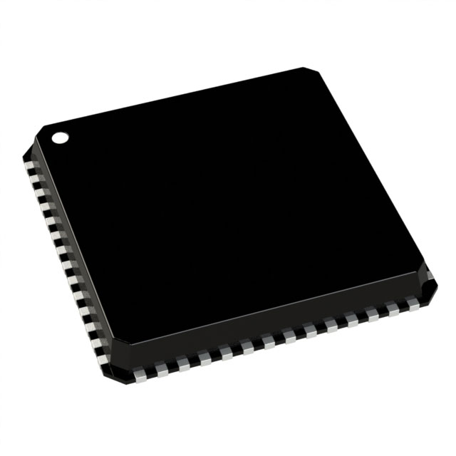
| Package / Case | 56-VFQFN Exposed Pad, CSP |
| Peripherals | PSM, Temp Sensor, DMA, WDT, PWM |
| Program Memory Type | FLASH |
| RAM Size | 2.25 K |
| Speed | 16.78 MHz |
| Supplier Device Package | 56-LFCSP-VQ (8x8) |
| Voltage - Supply (Vcc/Vdd) [Max] | 5.25 V |
| Voltage - Supply (Vcc/Vdd) [Min] | 4.75 V |
Pricing
Prices provided here are for design reference only. For realtime values and availability, please visit the distributors directly
| Distributor | Package | Quantity | $ | |
|---|---|---|---|---|
| Digikey | Bag | 34 | $ 8.98 | |
Description
General part information
ADuC843 Series
TheADuC841/ADuC842/ADuC843 are complete smart transducer front ends, that integrates a high performance self-calibrating multichannel ADC, a dual DAC, and an optimized single-cycle 20 MHz 8-bit MCU (8051 instruction set compatible) on a single chip.The ADuC841 and ADuC842 are identical with the exception of the clock oscillator circuit; the ADuC841 is clocked directly from an external crystal up to 20 MHz whereas the ADuC842 uses a 32 kHz crystal with an on-chip PLL generating a programmable core clock up to 16.78 MHz.The ADuC843 is identical to the ADuC842 except that the ADuC843 has no analog DAC outputs.The microcontroller is an optimized 8052 core offering up to 20 MIPS peak performance. Three different memory options are available offering up to 62 kBytes of nonvolatile Flash/EE program memory. Four kBytes of nonvolatile Flash/EE data memory, 256 bytes RAM, and 2 kBytes of extended RAM are also integrated on-chip.The parts also incorporate additional analog functionality with two 12-bit DACs, power supply monitor, and a band gap reference. On-chip digital peripherals include two 16-bit Σ-Δ. DACs, a dual output 16-bit PWM, a watchdog timer, a time interval counter, three timers/counters, and three serial I/O ports (SPI, I2C, and UART).On the ADuC812 and the ADuC832, the I2C and SPI interfaces share some of the same pins. For backwards compatibility, this is also the case for the ADuC841/ADuC842/ADuC843.However, there is also the option to allow SPI operate separately on P3.3, P3.4, and P3.5, while I2C uses the standard pins. The I2C interface has also been enhanced to offer repeated start, general call, and quad addressing.On-chip factory firmware supports in-circuit serial download and debug modes (via UART) as well as single-pin emulation mode via theEApin.ApplicationsOptical networking—laser power controlBase station systemsPrecision instrumentation, smart sensorsTransient capture systemsDAS and communications systems
Documents
Technical documentation and resources


