Deep-Dive with AI
Search across all available documentation for this part.

Deep-Dive with AI
Technical Specifications
Parameters and characteristics for this part
| Specification | HMC6545LP5ETR |
|---|---|
| Frequency [Max] | 32 GHz |
| Frequency [Min] | 0 Hz |
| Function | Linear Equalizer |
| Mounting Type | Surface Mount |
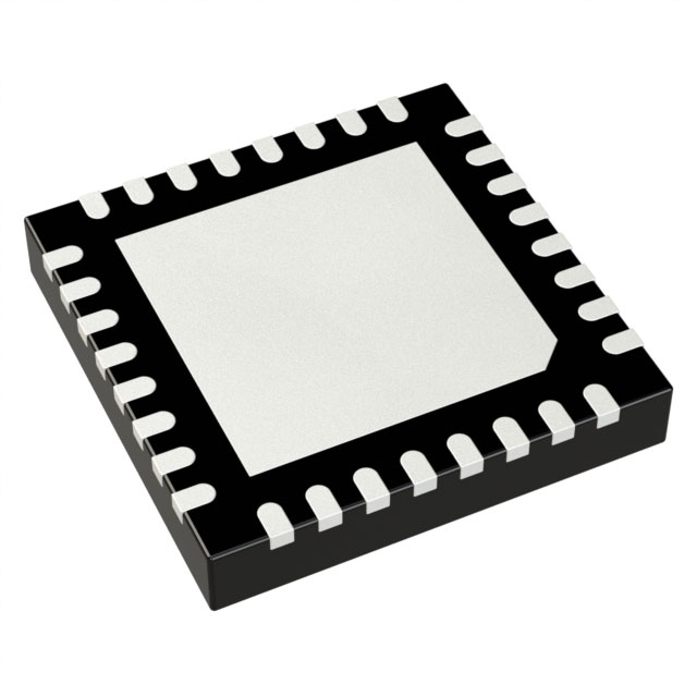
| Package / Case | 32-VFQFN Exposed Pad |
| RF Type | General Purpose |
| Supplier Device Package | 32-QFN (5x5) |
Pricing
Prices provided here are for design reference only. For realtime values and availability, please visit the distributors directly
| Distributor | Package | Quantity | $ | |
|---|---|---|---|---|
Description
General part information
HMC654-Die Series
The HMC6545 is a low power, high performance, fully programmable, dual-channel, asynchronous advanced linear equalizer that operates at data rates of up to 32 Gbps. The HMC6545 is protocol and data rate agnostic, and it can operate on the transmit path to predistort a transmitted signal to invert channel distortion or on the receiver path to equalize the distorted and attenuated received signal. The HMC6545 is effective in dealing with chromatic and polarization mode dispersion and intersymbol interference (ISI) caused by a wide variety of transmission media (backplane or fiber) and channel lengths.The HMC6545 consists of an automatic gain control (AGC); dc offset correction circuitry; a 9-tap, 18 ps spaced feedforward equalizer (FFE); a summing node; and a linear programmable output driver. The input AGC linearly attenuates or amplifies the distorted input signal to generate a constant voltage at the input of the FFE. The 9-tap FFE is programmed via 2-wire interface to generate wide range frequency responses that are precursor or postcursor in nature for compensating signal impairments. After FFE tap coefficients are summed at the summing node, the signal is received by a linear output driver. DC offset correction circuitry is controlled either automatically or manually via Forward Error Correction (FEC).All high speed differential inputs and outputs of the HMC6545 are current mode logic (CML) and terminated on chip with 50 Ω to the positive supply, 3.3 V, and can be dc-coupled or ac-coupled. The inputs and outputs of the HMC6545 can be operated either differentially or single-ended. The low power, high performance, and feature rich HMC6545 is packaged in a 5 mm × 5 mm, 32-lead LFCSP package. The device uses a single 3.3 V supply, eliminating external regulators. The HMC6545 operates over a −40°C to +95°C temperature range.Applications40 Gbps/100 Gbps DQPSK direct detection receiversShort and long reach CFP2 and QSFP+ modulesCEI-28G MR and CEI-25G LR 100 GE line cards16 Gbps and 32 Gbps Fibre ChannelInfiniband 14 Gbps FDR and 28 Gbps EDR ratesSignal conditioning for backplane and line cardsBroadband test and measurement equipment
Documents
Technical documentation and resources


