Deep-Dive with AI
Search across all available documentation for this part.

Deep-Dive with AI
Technical Specifications
Parameters and characteristics for this part
| Specification | AD565AJR |
|---|---|
| Architecture | R-2R |
| Data Interface | Parallel |
| Differential Output | False |
| INL/DNL (LSB) | 0.5 LSB |
| Mounting Type | Surface Mount |
| Number of Bits | 12 bits |
| Operating Temperature [Max] | 70 °C |
| Operating Temperature [Min] | 0 °C |
| Output Type | Current - Unbuffered |
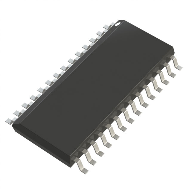
| Package / Case | 28-SOIC |
| Package / Case [x] | 0.295 in |
| Package / Case [y] | 7.5 mm |
| Reference Type | External, Internal |
| Settling Time | 400 ns |
| Supplier Device Package | 28-SOIC |
| Voltage - Supply, Analog [Max] | 16.5 V |
| Voltage - Supply, Analog [Min] | -11.4 V |
Pricing
Prices provided here are for design reference only. For realtime values and availability, please visit the distributors directly
| Distributor | Package | Quantity | $ | |
|---|---|---|---|---|
Description
General part information
JM38510/12103 Series
The AD565A and AD566A are fast 12-bit digital-to-analog converters which incorporate the latest advances in analog circuit design to achieve high speeds at low cost.The AD565A and AD566A use 12 precision, high-speed bipolar current-steering switches, control amplifier and a laser-trimmed thin-film resistor network to produce a very fast, high accuracy analog output current. The AD565A also includes a buried Zener reference that features low-noise, long-term stability and temperature drift characteristics comparable to the best discrete reference diodes.The combination of performance and flexibility in the AD565A and AD566A has resulted from major innovations in circuit design, an important new high-speed bipolar process, and continuing advances in laser-wafer-trimming techniques (LWT). The AD565A and AD566A have a 10-90% full-scale transition time less than 35 ns and settle to within ±1/2 LSB in 250 ns max (350 ns for AD566A). Both are laser-trimmed at the wafer level to ±1/8 LSB typical linearity and are specified to ±1/4 LSB max error (K and T grades) at +25°C. High speed and accuracy make the AD565A and AD566A the ideal choice for high-speed display drivers as well as fast analog-to-digital converters.The laser trimming process which provides the excellent linearity is also used to trim both the absolute value and the temperature coefficient of the reference of the AD565A resulting in a typical full-scale gain TC of 10 ppm/°C. When tighter TC performance is required or when a system reference is available, the AD566A may be used with an external reference.AD565A and AD566A are available in four performance grades. The J and K are specified for use over the 0°C to +70°C temperature range while the S and T grades are specified for the -55&176;C to +125°C range. The D grades are all packaged in a 24-pin, hermetically sealed, ceramic, dual-in-line package. The JR grade is packaged in a 28-pin plastic SOIC.
Documents
Technical documentation and resources


