Deep-Dive with AI
Search across all available documentation for this part.

Deep-Dive with AI
Technical Specifications
Parameters and characteristics for this part
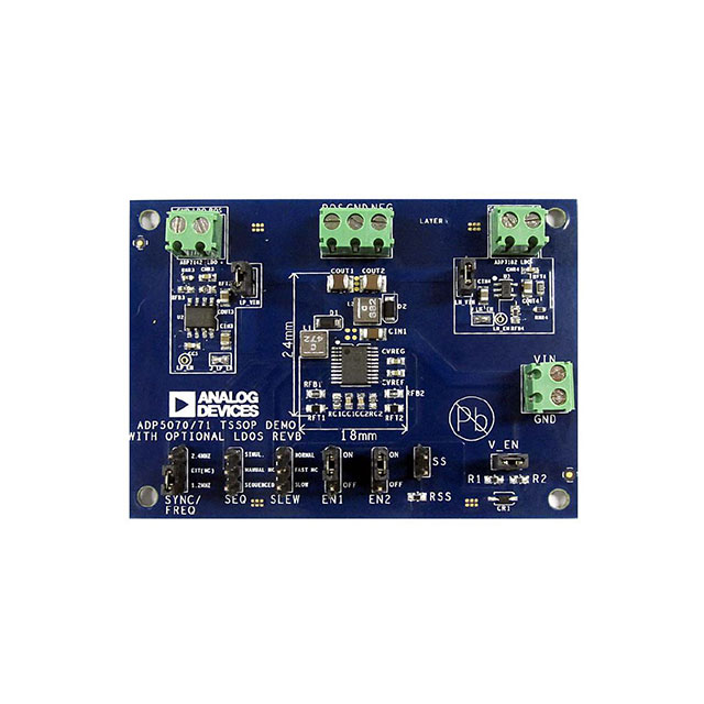
| Specification | ADP5070RE-EVALZ |
|---|---|
| Board Type | Fully Populated |
| Main Purpose | DC/DC, Step Up |
| Outputs and Type | 2 |
| Outputs and Type | Non-Isolated |
| Regulator Topology | Boost |
| Supplied Contents | Board(s) |
| Utilized IC / Part | ADP5070 |
| Voltage - Input [Max] | 5.5 V |
| Voltage - Input [Min] | 3 V |
| Voltage - Output | 15 V |
Pricing
Prices provided here are for design reference only. For realtime values and availability, please visit the distributors directly
| Distributor | Package | Quantity | $ | |
|---|---|---|---|---|
| Digikey | Box | 1 | $ 58.75 | |
Description
General part information
ADP5070 Series
TheADP5070is a dual high performance dc-to-dc regulator that generates independently regulated positive and negative rails.The input voltage range of 2.85 V to 15 V supports a wide variety of applications. The integrated main switch in both regulators enables generation of an adjustable positive output voltage up to +39 V and a negative output voltage down to −39 V below input voltage.The ADP5070 operates at a pin selected 1.2 MHz/2.4 MHz switching frequency. The ADP5070 can synchronize with an external oscillator from 1.0 MHz to 2.6 MHz to ease noise filtering in sensitive applications. Both regulators implement programmable slew rate control circuitry for the MOSFET driver stage to reduce electromagnetic interference (EMI).Flexible start-up sequencing is provided with the options of manual enable, simultaneous mode, positive supply first, and negative supply first.The ADP5070 includes a fixed internal or resistor programmable soft start timer to prevent inrush current at power-up. During shutdown, both regulators completely disconnect the loads from the input supply to provide a true shutdown.Other key safety features in the ADP5070 include overcurrent protection (OCP), overvoltage protection (OVP), thermal shutdown (TSD), and input undervoltage lockout (UVLO).The ADP5070 is available in a 20-lead LFCSP or in a 20-lead TSSOP and is rated for a −40°C to +125°C junction temperature range.ApplicationsBipolar amplifiers, ADCs, DACs and multiplexersCharge-coupled device (CCD) bias supplyOptical module supplyRF power amplifier (PA) bias
Documents
Technical documentation and resources


