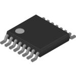
M74HC4094YTTR
ActiveSHIFT REGISTER/LATCH SINGLE 8-BIT SERIAL TO SERIAL/PARALLEL AUTOMOTIVE AEC-Q100 16-PIN TSSOP T/R

M74HC4094YTTR
ActiveSHIFT REGISTER/LATCH SINGLE 8-BIT SERIAL TO SERIAL/PARALLEL AUTOMOTIVE AEC-Q100 16-PIN TSSOP T/R
Technical Specifications
Parameters and characteristics for this part
| Specification | M74HC4094YTTR |
|---|---|
| Function | Serial to Parallel |
| Grade | Automotive |
| Logic Type | Shift Register |
| Mounting Type | Surface Mount |
| Number of Bits per Element [custom] | 8 |
| Number of Elements | 1 |
| Operating Temperature [Max] | 125 °C |
| Operating Temperature [Min] | -40 C |
| Output Type | Tri-State |
| Package / Case | 16-TSSOP |
| Package / Case [y] | 4.4 mm |
| Package / Case [y] | 0.173 in |
| Qualification | AEC-Q100 |
| Supplier Device Package | 16-TSSOP |
| Voltage - Supply [Max] | 6 V |
| Voltage - Supply [Min] | 2 V |
Pricing
Prices provided here are for design reference only. For realtime values and availability, please visit the distributors directly
Description
General part information
M74HC4094 Series
The M74HC4094 device is a high speed CMOS 8-bit SIPO shift latch register fabricated with silicon gate C2MOS technology. It consists of an 8-bit shift register and an 8-bit latch with 3-state output buffer. Data is shifted serially through the shift register on the positive going transition of the clock input signal. The output of the last stage (QS) can be used to cascade several devices.
Data on the QS output is transferred to a second output (QS’) on the following negative transition of the clock input signal. The data of each stage of the shift register is provided with a latch, which latches data on the negative going transition of the STROBE input signal. When the STROBE input is held high, data propagates through the latch to a 3-state output buffer. This buffer is enabled when OUTPUT ENABLE input is taken high. All inputs are equipped with protection circuits against static discharge and transient excess voltage.
Documents
Technical documentation and resources


