Deep-Dive with AI
Search across all available documentation for this part.

Deep-Dive with AI
Technical Specifications
Parameters and characteristics for this part
| Specification | AD8801AR |
|---|---|
| Architecture | R-2R |
| Data Interface | SPI |
| Differential Output | False |
| INL/DNL (LSB) | 0.25 LSB, 0.5 LSB |
| Mounting Type | Surface Mount |
| Number of Bits | 8 |
| Number of D/A Converters | 8 |
| Operating Temperature [Max] | 85 °C |
| Operating Temperature [Min] | -40 °C |
| Output Type | Voltage - Unbuffered |
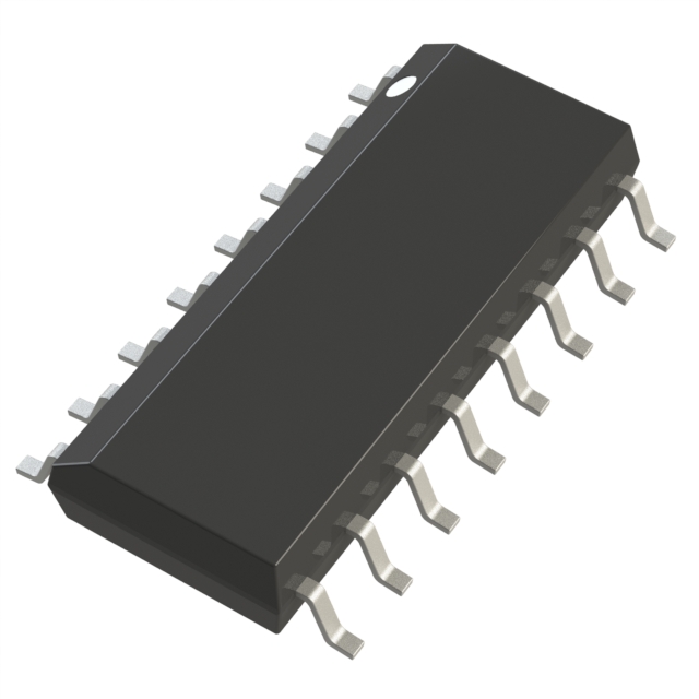
| Package / Case | 16-SOIC |
| Package / Case [x] | 0.154 in |
| Package / Case [y] | 3.9 mm |
| Reference Type | External |
| Settling Time | 600 ns |
| Supplier Device Package | 16-SOIC |
| Voltage - Supply, Analog [Max] | 5.5 V |
| Voltage - Supply, Analog [Min] | 2.7 V |
| Voltage - Supply, Digital [Max] | 5.5 V |
| Voltage - Supply, Digital [Min] | 2.7 V |
Pricing
Prices provided here are for design reference only. For realtime values and availability, please visit the distributors directly
| Distributor | Package | Quantity | $ | |
|---|---|---|---|---|
Description
General part information
AD8801 Series
The AD8801 /AD8803provides eight digitally controlled dc voltage outputs. This potentiometer divider TrimDAC®allows replacement of the mechanical trimmer function in new designs. The AD8801 / AD8803 is ideal for dc voltage adjustment applications.Easily programmed by serial interfaced microcontroller ports, the AD8801 with its midscale preset is ideal for potentiometer replacement where adjustments start at a nominal value. Applications such as gain control of video amplifiers, voltage controlled frequencies and bandwidths in video equipment, geometric correction and automatic adjustment in CRT computer graphic displays are a few of the many applications ideally suited for these parts. The AD8803 provides independent control of both the top and bottom end of the potentiometer divider allowing a separate zero-scale voltage setting determined by the VREFLpin. This is helpful for maximizing the resolution of devices with a limited allowable voltage control range.Internally the AD8801 / AD8803 contain eight voltage output digital-to-analog converters, sharing a common reference voltage input.Each DAC has its own DAC register that holds its output state. These DAC registers are updated from an internal serial-to-parallel shift register that is loaded from a standard three-wire serial input digital interface. Eleven data bits make up the data word clocked into the serial input register. This data word is decoded where the first 3 bits determine the address of the DAC register to be loaded with the last 8 bits of data. The AD8801 / AD8803 consumes only 5 mA from 5 V power supplies. In addition, in shutdown mode reference input current consumption is also reduced to 5 µA while saving the DAC latch settings for use after return to normal operation.The AD8801 / AD8803 is available in 16-pin plastic DIP and the 1.5 mm height SO-16 surface mount packages.
Documents
Technical documentation and resources


