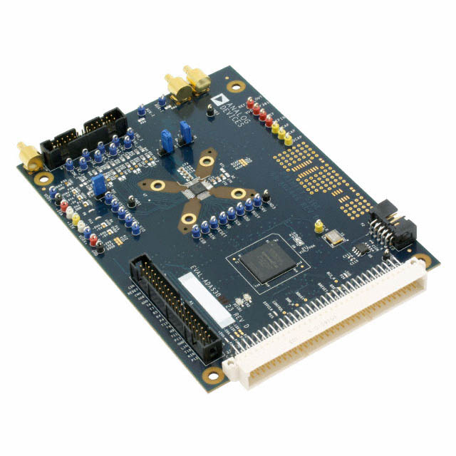

Technical Specifications
Parameters and characteristics for this part
| Specification | EVAL-ADAS3023EDZ |
|---|---|
| Data Interface | SPI |
| Input Range | 0.3 V |
| Number of A/D Converters | 1 |
| Number of Bits | 16 |
| Sampling Rate (Per Second) | 1 M |
| Supplied Contents | Board(s) |
| Utilized IC / Part | ADAS3023 |
Pricing
Prices provided here are for design reference only. For realtime values and availability, please visit the distributors directly
| Distributor | Package | Quantity | $ | |
|---|---|---|---|---|
| Digikey | Box | 1 | $ 104.88 | |
Description
General part information
ADAS3023 Series
The ADAS3023 is a complete 16-bit, successive approximation-based, analog-to-digital data acquisition system. This device is capable of simultaneously sampling up to 500 kSPS for two channels, 250 kSPS for four channels, 167 kSPS for six channels, and 125 kSPS for eight channels, and manufactured on the Analog Devices, Inc., proprietaryiCMOS®high voltage industrial process technology.The ADAS3023 integrates eight channels of low leakage track-and-hold design, a programmable gain instrumentation amplifier (PGIA) stage with a high common-mode rejection offering four differential input ranges, a precision low drift 4.096 V reference and buffer, and a 16-bit charge redistribution PulSAR®successive approximation register (SAR) analog-to-digital converter (ADC). The ADAS3023 is factory calibrated and can resolve differential input ranges of up to ±20.48 V when using ±15 V supplies.The ADAS3023 simplifies design challenges by eliminating signal buffering, level shifting, amplification and attenuation, common-mode rejection, settling time, or any of the other analog signal conditioning challenges, and allows smaller form factor, faster time to market, and lower costs.The ADAS3023 is available in a 40-lead LFCSP with operation specified from −40°C to +85°C.
Documents
Technical documentation and resources


